Datasheet 搜索 > 二极管阵列 > Vishay Semiconductor(威世) > VS-12CWQ04FNTRLPBF 数据手册 > VS-12CWQ04FNTRLPBF 数据手册 1/7 页

¥ 0.582
VS-12CWQ04FNTRLPBF 数据手册 - Vishay Semiconductor(威世)
制造商:
Vishay Semiconductor(威世)
分类:
二极管阵列
封装:
TO-252-3
描述:
肖特基整流器, 2× 6的大众D- PAK大纲 Schottky Rectifier, 2 x 6 A Popular D-PAK outline
Pictures:
3D模型
符号图
焊盘图
引脚图
产品图
VS-12CWQ04FNTRLPBF数据手册
Page:
of 7 Go
若手册格式错乱,请下载阅览PDF原文件
Document Number: 94133 For technical questions within your region, please contact one of the following: www.vishay.com
Revision: 14-Jan-11 DiodesAmericas@vishay.com
, DiodesAsia@vishay.com, DiodesEurope@vishay.com 1
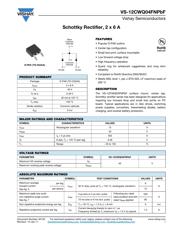
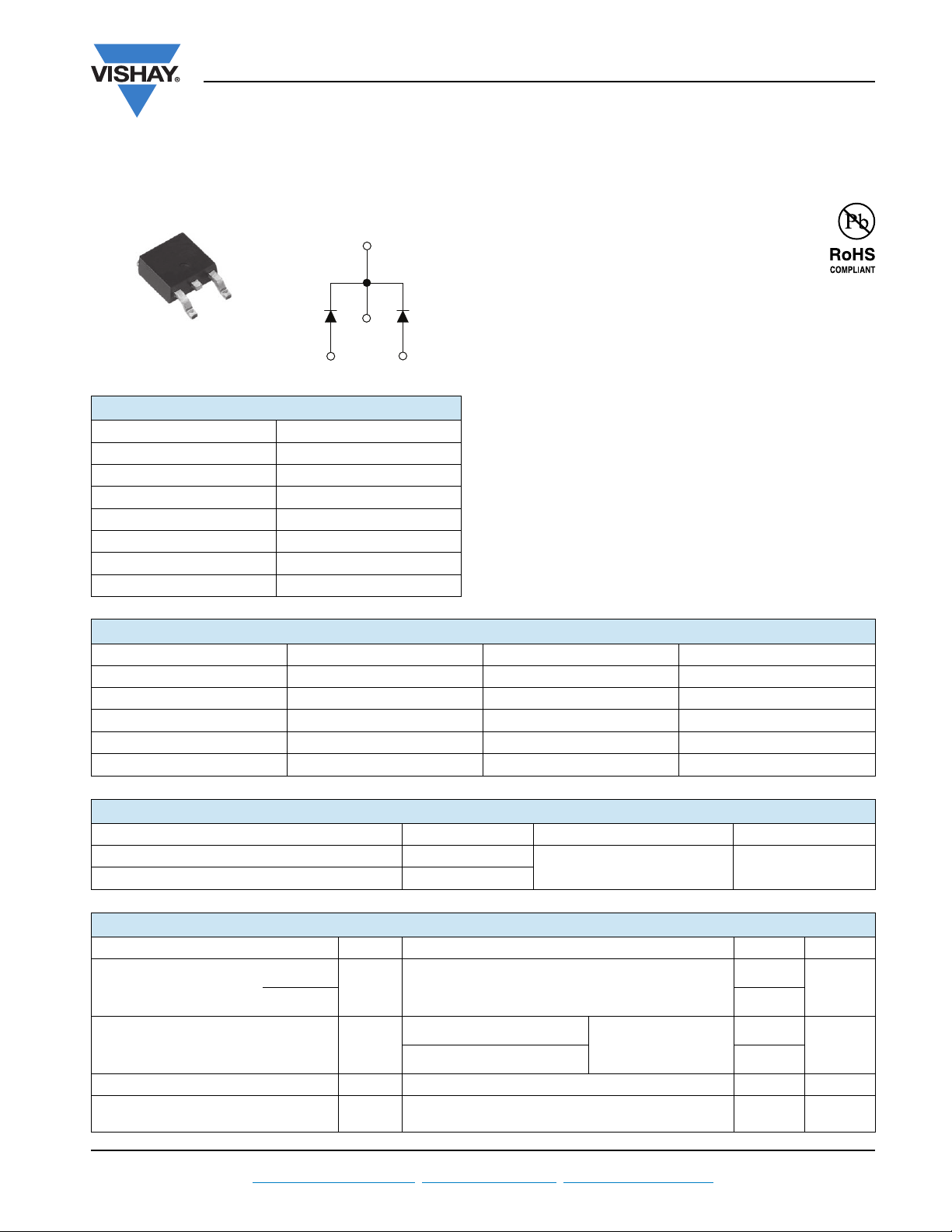
Schottky Rectifier, 2 x 6 A
VS-12CWQ04FNPbF
Vishay Semiconductors
FEATURES
• Popular D-PAK outline
• Center tap configuration
• Small foot print, surface mountable
• Low forward voltage drop
• High frequency operation
• Guard ring for enhanced ruggedness and long term
reliability
• Compliant to RoHS Directive 2002/95/EC
• Meets MSL level 1, per J-STD-020, LF maximum peak of
260 °C
DESCRIPTION
The VS-12CWQ04FNPbF surface mount, center tap,
Schottky rectifier series has been designed for applications
requiring low forward drop and small foot prints on PC
board. Typical applications are in disk drives, switching
power supplies, converters, freewheeling diodes, battery
charging, and reverse battery protection.
PRODUCT SUMMARY
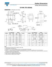
Package D-PAK (TO-252AA)
I
F(AV)
2 x 6 A
V
R
40 V
V
F
at I
F
0.48 V
I
RM
40 mA at 125 °C
T
J
max. 150 °C
Diode variation Common cathode
E
AS
9 mJ
Base
common
cathode
Common
cathode
2
4
13
Anode Anode
D-PAK (TO-252AA)
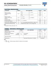
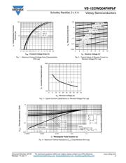
MAJOR RATINGS AND CHARACTERISTICS
SYMBOL CHARACTERISTICS VALUES UNITS
I
F(AV)
Rectangular waveform 12 A
V
RRM
40 V
I
FSM
t
p
= 5 μs sine 550 A
V
F
6 Apk, T
J
= 125 °C (per leg) 0.48 V
T
J
Range - 55 to 150 °C
VOLTAGE RATINGS
PARAMETER SYMBOL VS-12CWQ04FNPbF UNITS
Maximum DC reverse voltage V
R
40 V
Maximum working peak reverse voltage V
RWM
ABSOLUTE MAXIMUM RATINGS
PARAMETER SYMBOL TEST CONDITIONS VALUES UNITS
Maximum average
forward current
See fig. 5
per leg
I
F(AV)
50 % duty cycle at T
C
= 134 °C, rectangular waveform
6
A
per device 12
Maximum peak one cycle
non-repetitive surge current
See fig. 7
I
FSM
5 μs sine or 3 μs rect. pulse
Following any rated
load condition and with
rated V
RRM
applied
550
A
10 ms sine or 6 ms rect. pulse 90
Non-repetitive avalanche energy per leg E
AS
T
J
= 25 °C, I
AS
= 1.5 A, L = 8 mH 9 mJ
Repetitive avalanche current per leg I
AR
Current decaying linearly to zero in 1 μs
Frequency limited by T
J
maximum V
A
= 1.5 x V
R
typical
1.2 A
器件 Datasheet 文档搜索
AiEMA 数据库涵盖高达 72,405,303 个元件的数据手册,每天更新 5,000 多个 PDF 文件
