Datasheet 搜索 > EEPROM芯片 > Xilinx(赛灵思) > XC18V04PC44C 数据手册 > XC18V04PC44C 数据手册 1/25 页
 器件3D模型
¥ 9.1
XC18V04PC44C 数据手册 - Xilinx(赛灵思)
制造商:
Xilinx(赛灵思)
分类:
EEPROM芯片
封装:
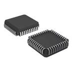
PLCC-44
描述:
XC18V04PC44C 磨码
Pictures:
3D模型
符号图
焊盘图
引脚图
产品图
页面导航:
导航目录
XC18V04PC44C数据手册
Page:
of 25 Go
若手册格式错乱,请下载阅览PDF原文件
DS026 (v6.0) August 5, 2015 www.xilinx.com
Product Specification 1
© 1999–2008, 2015 Xilinx, Inc. Xilinx, the Xilinx logo, Artix, ISE, Kintex, Spartan, Virtex, Vivado, Zynq, and other designated brands included herein are trademarks of Xilinx in
the United States and other countries.
— PRODUCT OBSOLETE / UNDER OBSOLESCENCE —
Features
• In-System Programmable 3.3V PROMs for
Configuration of Xilinx FPGAs
♦ Endurance of 20,000 Program/Erase Cycles
♦ Program/Erase Over Full Industrial Voltage and
Temperature Range (–40
°C to +85°C)
• IEEE Std 1149.1 Boundary-Scan (JTAG) Support
• JTAG Command Initiation of Standard FPGA
Configuration
• Simple Interface to the FPGA
• Cascadable for Storing Longer or Multiple Bitstreams
• Low-Power Advanced CMOS FLASH Process
• Dual Configuration Modes
♦ Serial Slow/Fast Configuration (up to 33 MHz)
♦ Parallel (up to 264 Mb/s at 33 MHz)
• 5V-Tolerant I/O Pins Accept 5V, 3.3V and 2.5V Signals
• 3.3V or 2.5V Output Capability
• Design Support Using the Xilinx ISE™ Foundation™
Software Packages
• Available in PC20, SO20, PC44, and VQ44 Packages
• Lead-Free (Pb-Free) Packaging
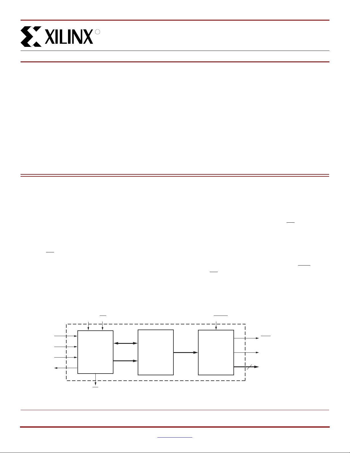
Description
Xilinx introduces the XC18V00 series of in-system
programmable configuration PROMs (Figure 1). Devices in
this 3.3V family include a 4-megabit, a 2-megabit, a
1-megabit, and a 512-kilobit PROM that provide an easy-to-
use, cost-effective method for reprogramming and storing
Xilinx FPGA configuration bitstreams.
When the FPGA is in Master Serial mode, it generates a
configuration clock that drives the PROM. A short access
time after CE
and OE are enabled, data is available on the
PROM DATA (D0) pin that is connected to the FPGA DIN
pin. New data is available a short access time after each
rising clock edge. The FPGA generates the appropriate
number of clock pulses to complete the configuration. When
the FPGA is in Slave Serial mode, the PROM and the FPGA
are clocked by an external clock.
When the FPGA is in Master SelectMAP mode, the FPGA
generates a configuration clock that drives the PROM. When
the FPGA is in Slave Parallel or Slave SelectMAP mode, an
external oscillator generates the configuration clock that
drives the PROM and the FPGA. After CE
and OE are
enabled, data is available on the PROM’s DATA (D0-D7)
pins. New data is available a short access time after each
rising clock edge. The data is clocked into the FPGA on the
following rising edge of the CCLK. A free-running oscillator
can be used in the Slave Parallel or Slave SelecMAP modes.
Multiple devices can be cascaded by using the CEO
output
to drive the CE
input of the following device. The clock
inputs and the DATA outputs of all PROMs in this chain are
interconnected. All devices are compatible and can be
cascaded with other members of the family or with the
XC17V00 one-time programmable serial PROM family.
25
XC18V00 Series In-System-Programmable
Configuration PROMs
DS026 (v6.0) August 5, 2015
0
Product Specification
R
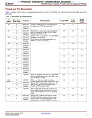
X-Ref Target - Figure 1
Figure 1: XC18V00 Series Block Diagram
Control
and
JTAG
Interface
Memory
Serial
or
Parallel
Interface
D0 DATA
Serial or Parallel Mode
D[1:7]
Parallel Interface
Data
Address
CLK CE
TCK
TMS
TDI
TDO
OE/RESET
CEO
Data
DS026_01_040204
7
CF
器件 Datasheet 文档搜索
AiEMA 数据库涵盖高达 72,405,303 个元件的数据手册,每天更新 5,000 多个 PDF 文件
