Datasheet 搜索 > CPLD芯片 > Xilinx(赛灵思) > XC2C256-6VQG100C 数据手册 > XC2C256-6VQG100C 数据手册 1/16 页
 器件3D模型
¥ 12.968
XC2C256-6VQG100C 数据手册 - Xilinx(赛灵思)
制造商:
Xilinx(赛灵思)
分类:
CPLD芯片
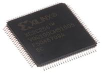
封装:
TQFP-100
描述:
Xilinx### 复杂可编程逻辑器件 (CPLD)
Pictures:
3D模型
符号图
焊盘图
引脚图
产品图
页面导航:
原理图在P6
封装信息在P14
技术参数、封装参数在P14
应用领域在P14


导航目录
XC2C256-6VQG100C数据手册
Page:
of 16 Go
若手册格式错乱,请下载阅览PDF原文件
DS090 (v3.1) September 11, 2008 www.xilinx.com 1
Product Specification
© 2002–2008 Xilinx, Inc. All rights reserved. All Xilinx trademarks, registered trademarks, patents, and disclaimers are as listed at http://www.xilinx.com/legal.htm.
All other trademarks and registered trademarks are the property of their respective owners. All specifications are subject to change without notice.
Features
• Optimized for 1.8V systems
- Industry’s fastest low power CPLD
- Densities from 32 to 512 macrocells
• Industry’s best 0.18 micron CMOS CPLD
- Optimized architecture for effective logic synthesis
- Multi-voltage I/O operation — 1.5V to 3.3V
• Advanced system features
- Fastest in system programming
· 1.8V ISP using IEEE 1532 (JTAG) interface
- On-The-Fly Reconfiguration (OTF)
- IEEE1149.1 JTAG Boundary Scan Test
- Optional Schmitt trigger input (per pin)
- Multiple I/O banks on all devices
- Unsurpassed low power management
· DataGATE external signal control
- Flexible clocking modes
· Optional DualEDGE triggered registers
· Clock divider (÷ 2,4,6,8,10,12,14,16)
· CoolCLOCK
- Global signal options with macrocell control
· Multiple global clocks with phase selection per
macrocell
· Multiple global output enables
· Global set/reset
- Abundant product term clocks, output enables and
set/resets
- Efficient control term clocks, output enables and
set/resets for each macrocell and shared across
function blocks
- Advanced design security
- Open-drain output option for Wired-OR and LED
drive
- Optional bus-hold, 3-state or weak pullup on select
I/O pins
- Optional configurable grounds on unused I/Os
- Mixed I/O voltages compatible with 1.5V, 1.8V,
2.5V, and 3.3V logic levels on all parts
- SSTL2_1,SSTL3_1, and HSTL_1 on 128
macrocell and denser devices
- Hot pluggable
• PLA architecture
- Superior pinout retention
- 100% product term routability across function block
• Wide package availability including fine pitch:
- Chip Scale Package (CSP) BGA, Fine Line BGA,
TQFP, PQFP, VQFP, and QFN packages
- Pb-free available for all packages
• Design entry/verification using Xilinx and industry
standard CAE tools
• Free software support for all densities using Xilinx®
WebPACK™ tool
• Industry leading nonvolatile 0.18 micron CMOS
process
- Guaranteed 1,000 program/erase cycles
- Guaranteed 20 year data retention
Family Overview
Xilinx CoolRunner™-II CPLDs deliver the high speed and
ease of use associated with the XC9500/XL/XV CPLD fam-
ily with the extremely low power versatility of the XPLA3
family in a single CPLD. This means that the exact same
parts can be used for high-speed data communications/
computing systems and leading edge portable products,
with the added benefit of In System Programming. Low
power consumption and high-speed operation are com-
bined into a single family that is easy to use and cost effec-
tive. Clocking techniques and other power saving features
extend the users’ power budget. The design features are
supported starting with Xilinx ISE® 4.1i WebPACK tool.
Additional details can be found in Further Reading,
page 14.
Table 1 shows the macrocell capacity and key timing
parameters for the CoolRunner-II CPLD family.
0
CoolRunner-II CPLD Family
DS090 (v3.1) September 11, 2008
00
Product Specification
R
Table 1: CoolRunner-II CPLD Family Parameters
XC2C32A XC2C64A XC2C128 XC2C256 XC2C384 XC2C512
Macrocells 32 64 128 256 384 512
Max I/O 33 64 100 184 240 270
T
PD
(ns) 3.8 4.6 5.7 5.7 7.1 7.1
T
SU
(ns) 1.9 2.0 2.4 2.4 2.9 2.6
T
CO
(ns) 3.7 3.9 4.2 4.5 5.8 5.8
F
SYSTEM1
(MHz) 323 263 244 256 217 179
器件 Datasheet 文档搜索
AiEMA 数据库涵盖高达 72,405,303 个元件的数据手册,每天更新 5,000 多个 PDF 文件
