Datasheet 搜索 > 开发套件 > Zentrum Mikroelektronik Dresden > ZSC31050KIT 数据手册 > ZSC31050KIT 数据手册 12/28 页

¥ 1574.022
ZSC31050KIT 数据手册 - Zentrum Mikroelektronik Dresden
制造商:
Zentrum Mikroelektronik Dresden
分类:
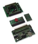
开发套件
Pictures:
3D模型
符号图
焊盘图
引脚图
产品图
页面导航:

导航目录
ZSC31050KIT数据手册
Page:
of 28 Go
若手册格式错乱,请下载阅览PDF原文件
ZSC31050
Advanced Differential Sensor Signal Conditioner
Data Sheet
July 29, 2010
© 2010 Zentrum Mikroelektronik Dresden AG — Rev. 1.11
All rights reserved. The material contained herein may not be reproduced, adapted, merged, translated, stored, or used without
the prior written consent of the copyright owner. The information furnished in this publication is subject to changes without
notice.
12 of 28
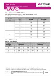
2 Circuit Description
2.1. Signal Flow
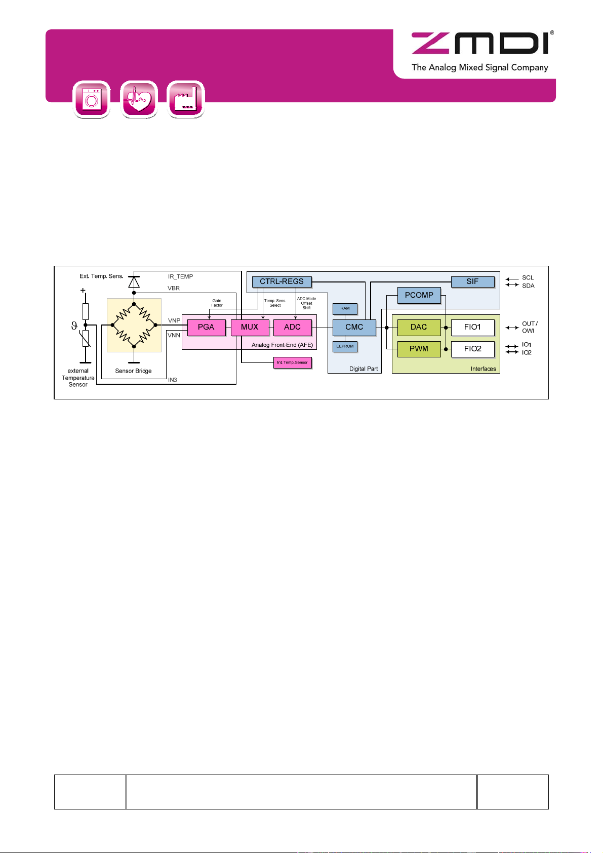
The ZSC31050’s signal path is partly analog (blue) and partly digital (red). The analog part is realized
differential – this means internal is the differential bridge sensor signal also handled via two signal lines, which
are rejected symmetrically around a common mode potential (analog ground = VDDA/2).
Consequently it is possible to amplify positive and negative input signals, which are located in the common
mode range of the signal input.
Figure 2.1 Block Diagram of the ZSC31050
The differential signal from the bridge sensor is pre-amplified by the programmable gain amplifier (PGA). The
Multiplexer (MUX) transmits the signals from bridge sensor, external diode or separate temperature sensor to
the ADC in a certain sequence (instead of the temperature diode the internal pn-junction (TS) can be used
optionally). Afterwards the ADC converts these signals into digital values.
The digital signal correction takes place in the calibration micro-controller (CMC). It is based on a special
correction formula located in the ROM and on sensor-specific coefficients (stored into the EEPROM during
calibration). Dependent on the programmed output configuration the corrected sensor signal is output as
analog value, as PWM signal or in digital format (SPI, I
2
C and ZACwire
TM
). The output signal is provided at 2
flexible I/O modules (FIO) and at the serial interface (SIF). The configuration data and the correction
parameters can be programmed into the EEPROM via the digital interfaces.
PGA Programmable Gain Amplifier
MUX Multiplexer
ADC Analog-to-Digital Converter
CMC Calibration Microcontroller
DAC Digital-to-Analog Converter
FIO1 Flexible I/O 1: Analog Out (voltage/current), PWM2, ZACwire
TM
(one-wire-interface)
FIO2 Flexible I/O 2: PWM1, SPI Data Out, SPI Slave Select, Alarm1, Alarm2
SIF Serial interface: I
2
C Data I/O, SPI Data In, Clock
PCOMP Programmable Comparator
EEPROM Non Volatile Memory for Calibration Parameters and Configuration
TS On-chip Temperature Sensor (pn-junction)
ROM Memory for Correction Formula and –Algorithm
PWM PWM Module
器件 Datasheet 文档搜索
AiEMA 数据库涵盖高达 72,405,303 个元件的数据手册,每天更新 5,000 多个 PDF 文件
