Datasheet 搜索 > Zetex > ZVN3310ASTOA 数据手册 > ZVN3310ASTOA 数据手册 2/3 页

¥ 0
ZVN3310ASTOA 数据手册 - Zetex
制造商:
Zetex
Pictures:
3D模型
符号图
焊盘图
引脚图
产品图
页面导航:
技术参数、封装参数在P1P2
电气规格在P1P2

导航目录
ZVN3310ASTOA数据手册
Page:
of 3 Go
若手册格式错乱,请下载阅览PDF原文件
N-CHANNEL ENHANCEMENT
MODE VERTICAL DMOS FET
ISSUE 2 – MARCH 94
FEATURES
* 100 Volt V
DS
*R
DS(on)
= 10Ω
ABSOLUTE MAXIMUM RATINGS.
PARAMETER SYMBOL VALUE UNIT
Drain-Source Voltage V
DS
100 V
Continuous Drain Current at T
amb
=25°C I
D
200 mA
Pulsed Drain Current I
DM
2A
Gate-Source Voltage V
GS
± 20
V
Power Dissipation at T
amb
=25°C P
tot
625 mW
Operating and Storage Temperature Range T
j
:T
stg
-55 to +150 °C
ELECTRICAL CHARACTERISTICS (at T
amb
= 25°C unless otherwise stated).
PARAMETER SYMBOL MIN. MAX. UNIT CONDITIONS.
Drain-Source Breakdown
Voltage
BV
DSS
100 V I
D
=1mA, V
GS
=0V
Gate-Source Threshold
Voltage
V
GS(th)
0.8 2.4 V ID=1mA, V
DS
= V
GS
Gate-Body Leakage I
GSS
20 nA
V
GS
=± 20V, V
DS
=0V
Zero Gate Voltage Drain
Current
I
DSS
1
50
µA
µA
V
DS
=100V, V
GS
=0
V
DS
=80V, V
GS
=0V, T=125°C(2)
On-State Drain Current(1) I
D(on)
500 mA V
DS
=25V, V
GS
=10V
Static Drain-Source On-State
Resistance (1)
R
DS(on)
10
Ω
V
GS
=10V,I
D
=500mA
Forward Transconductance(1)(2
)
g
fs
100 mS V
DS
=25V,I
D
=500mA
Input Capacitance (2) C
iss
40 pF
Common Source Output
Capacitance (2)
C
oss
15 pF V
DS
=25V, V
GS
=0V, f=1MHz
Reverse Transfer Capacitance
(2)
C
rss
5pF
Turn-On Delay Time (2)(3) t
d(on)
5ns
V
DD
≈25V, I
D
=500mA
Rise Time (2)(3) t
r
7ns
Turn-Off Delay Time (2)(3) t
d(off)
6ns
Fall Time (2)(3) t
f
7ns
E-Line
TO92 Compatible
ZVN3310A
3-378
D
G
S
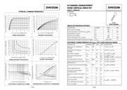
TYPICAL CHARACTERISTICS
Output Characteristics
VDS - Drain Source Voltage (Volts)
I
D(
O
n
)
-
On-
Stat
e
Drain Cur
r
e
n
t (
Am
ps)
Transfer Characteristics
0246810
0102030 40 50
Saturation Characteristics
6
0
2
4
8
04 8 121620
10
V
DS-
Drain Source
Voltage (Volts)
Voltage Saturation Characteristics
VGS-Gate Source Voltage (Volts)
5V
ID=
1A
0.5A
0.2A
I
D(
O
n
)
-
On-Sta
t
e D
r
ain
Current (Amp
s
)
VGS-Gate Source Voltage (Volts)
1.4
1.2
0.8
0.2
0
0.4
1.0
0.6
VGS=
10V
7V
8V
I
D(O
n
)
-On-State Drain Current (Amps)
VDS - Drain Source Voltage (Volts)
On-resistance vs gate-source voltage
VGS-Gate Source Voltage (Volts)
R
DS(ON)
-Drain Source Resistance
(
Ω
)
1234567891020
6V
4V
3V
1.6
1.2
0.4
0
0.8
0246810
1.4
1.2
0.8
0.2
0
0.4
1.0
0.6
VDS=
25V
9V
1.4
1.0
0.6
0.2
5V
VGS=
10V
7V
8V
6V
4V
3V
9V
I
D=
1A
0.5A
0.2A
1
10
100
Normalised R
DS(on)
and V
GS(th)
vs Temperature
Normalised R
DS(
o
n)
a
n
d V
GS(th)
-40
-20 0 20 40 60 80
120
100 140 160
2.4
2.2
2.0
1.8
1.6
1.4
1.2
1.0
0.6
0.8
Drai
n
-
S
o
u
rce
R
esi
s
ta
n
c
e R
DS(
o
n
)
G
ate
T
h
res
h
o
l
d
V
o
lt
ag
e
V
GS
(
th
)
ID=-0.5A
T-Temperature (C°)
0.4
-80
-60
ZVN3310A
3-379
器件 Datasheet 文档搜索
AiEMA 数据库涵盖高达 72,405,303 个元件的数据手册,每天更新 5,000 多个 PDF 文件
