Datasheet 搜索 > 陶瓷电容 > AVX(艾维克斯) > 04023A101JAT2A 数据手册 > 04023A101JAT2A 其他数据使用手册 2/4 页
 器件3D模型
¥ 0.247
04023A101JAT2A 其他数据使用手册 - AVX(艾维克斯)
制造商:
AVX(艾维克斯)
分类:
陶瓷电容
封装:
0402
描述:
AVX 04023A101JAT2A 多层陶瓷电容器, 表面贴装, 100 pF, ± 5%, C0G / NP0, 25 V, 0402 [1005 公制]
Pictures:
3D模型
符号图
焊盘图
引脚图
产品图
页面导航:
封装信息在P1P3P4
型号编号列表在P1

导航目录
04023A101JAT2A数据手册
Page:
of 4 Go
若手册格式错乱,请下载阅览PDF原文件
The Important Information/Disclaimer is incorporated in the catalog where these specications came from or
available online at www.avx.com/disclaimer/ by reference and should be reviewed in full before placing any order.
4
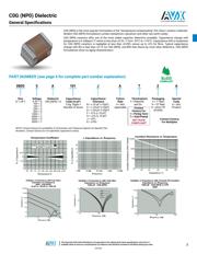
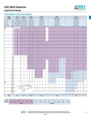
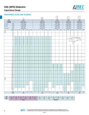
C0G (NP0) Dielectric
Specications and Test Methods
Parameter/Test NP0 Specication Limits Measuring Conditions
Operating Temperature Range -55ºC to +125ºC Temperature Cycle Chamber
Capacitance Within specied tolerance
<30 pF: Q≥ 400+20 x Cap Value
≥30 pF: Q≥ 1000
Freq.: 1.0 MHz ± 10% for cap ≤ 1000 pF
1.0 kHz ± 10% for cap > 1000 pF
Voltage: 1.0Vrms ± .2V
Q
Insulation Resistance
100,000MΩ or 1000MΩ - µF,
whichever is less
Charge device with rated voltage for 60 ± 5 secs
@ room temp/humidity
Dielectric Strength No breakdown or visual defects
Charge device with 250% of rated voltage for 1-5
seconds, w/charge and discharge current limited
to 50 mA (max)
Note: Charge device with 150% of rated voltage
for 500V devices.
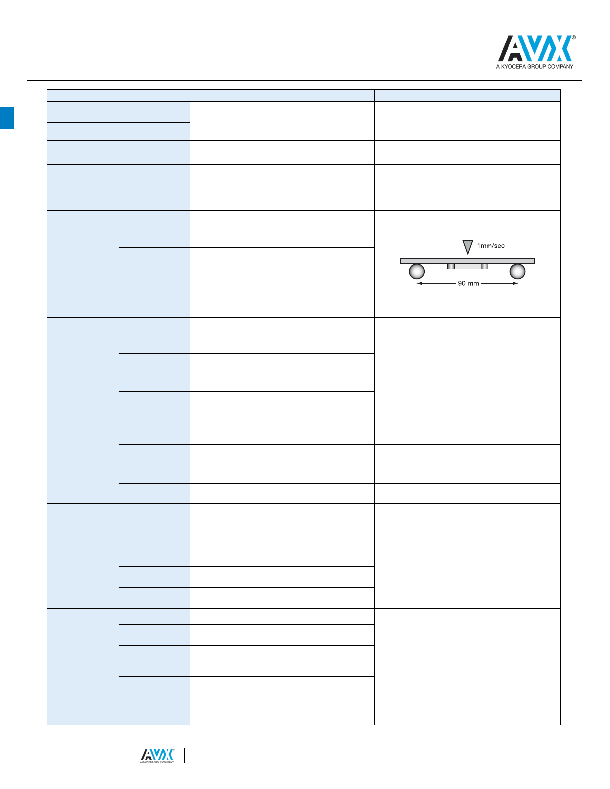
Resistance to
Flexure
Stresses
Appearance No defects
Deection: 2mm
Test Time: 30 seconds
Capacitance
Variation
±5% or ±.5 pF, whichever is greater
Q Meets Initial Values (As Above)
Insulation
Resistance
≥ Initial Value x 0.3
Solderability
≥ 95% of each terminal should be covered
with fresh solder
Dip device in eutectic solder at 230 ± 5ºC for 5.0 ±
0.5 seconds
Resistance to
Solder Heat
Appearance No defects, <25% leaching of either end terminal
Dip device in eutectic solder at 260ºC for
60sec- onds. Store at room temperature
for 24 ± 2hours before measuring electrical
properties.
Capacitance
Variation
≤ ±2.5% or ±.25 pF, whichever is greater
Q Meets Initial Values (As Above)
Insulation
Resistance
Meets Initial Values (As Above)
Dielectric
Strength
Meets Initial Values (As Above)
Thermal Shock
Appearance No visual defects Step 1: -55ºC ± 2º 30 ± 3 minutes
Capacitance
Variation
≤ ±2.5% or ±.25 pF, whichever is greater Step 2: Room Temp ≤ 3 minutes
Q Meets Initial Values (As Above) Step 3: +125ºC ± 2º 30 ± 3 minutes
Insulation
Resistance
Meets Initial Values (As Above) Step 4: Room Temp ≤ 3 minutes
Dielectric
Strength
Meets Initial Values (As Above)
Repeat for 5 cycles and measure after
24 hours at room temperature
Load Life
Appearance No visual defects
Charge device with twice rated voltage in test
chamber set at 125ºC ± 2ºC
for 1000 hours (+48, -0).
Remove from test chamber and stabilize at
room temperature for 24 hours
before measuring.
Capacitance
Variation
≤ ±3.0% or ± .3 pF, whichever is greater
Q
(C=Nominal Cap)
≥ 30 pF: Q≥ 350
≥10 pF, <30 pF: Q≥ 275 +5C/2
<10 pF: Q≥ 200 +10C
Insulation
Resistance
≥ Initial Value x 0.3 (See Above)
Dielectric
Strength
Meets Initial Values (As Above)
Load
Humidity
Appearance No visual defects
Store in a test chamber set at 85ºC ± 2ºC/ 85% ±
5% relative humidity for 1000 hours
(+48, -0) with rated voltage applied.
Remove from chamber and stabilize at room
temperature for 24 ± 2 hours before measuring.
Capacitance
Variation
≤ ±5.0% or ± .5 pF, whichever is greater
Q
≥ 30 pF: Q≥ 350
≥10 pF, <30 pF: Q≥ 275 +5C/2
<10 pF: Q≥ 200 +10C
Insulation
Resistance ≥ Initial Value x 0.3 (See Above)
Dielectric
Strength
Meets Initial Values (As Above)
051818
器件 Datasheet 文档搜索
AiEMA 数据库涵盖高达 72,405,303 个元件的数据手册,每天更新 5,000 多个 PDF 文件
