Datasheet 搜索 > 齐纳二极管 > Microsemi(美高森美) > 1N5357CE3/TR12 数据手册 > 1N5357CE3/TR12 其他数据使用手册 2/3 页

¥ 17.159
1N5357CE3/TR12 其他数据使用手册 - Microsemi(美高森美)
制造商:
Microsemi(美高森美)
分类:
齐纳二极管
封装:
T-18
Pictures:
3D模型
符号图
焊盘图
引脚图
产品图
1N5357CE3/TR12数据手册
Page:
of 3 Go
若手册格式错乱,请下载阅览PDF原文件

Summer 1997
13
Series 205
deviating from their nominal rating
at 7.5 mA is shown in Figure 1.
Also additional voltage changes
from dynamic impedance effects
must also be considered in such
applications where operating
current is not held relatively
constant as shown in Figure 2. It
should be apparent for applications
requiring very small voltage
changes that a well controlled
constant current source is desired
for optimum reference voltage
performance.
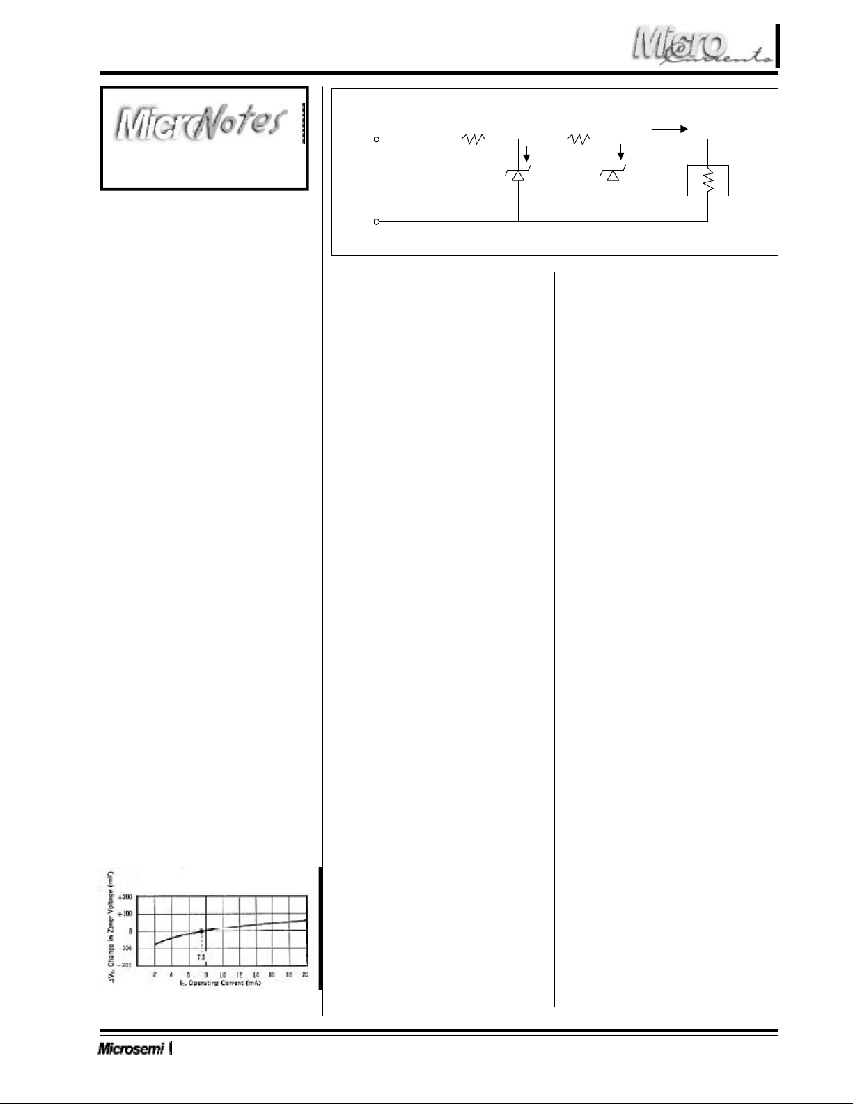
An example method of improving
constant current regulation to a
reference diode is shown in Figure
3. An initial zener of higher voltage
V
Z1
compared to a reference diode
V
Z2
offers improved current control
to the latter. Note that I
Z2
for the
reference diode is then determined
as I
Z2
= (V
Z1
- V
Z2
)/R
S2
where
comparatively small operating
current I
Z2
changes occur despite
notable changes in source voltage
V
S
. The current I
Z1
for the first
stage zener V
Z1
is determined as in
MicroNote 201 as I
Z1
= (V
S
- V
Z1
)/
R
S1
.
The circuit shown in Figure 3 is
particularly useful when voltage
changes in line source (V
S
) would
otherwise cause excessive current
fluctuations to the reference diode
V
Z2
. The zener voltage regulator V
Z1
must be greater than V
Z2
when
selecting R
S2
so that desired
operating current of the reference
diode I
Z2
= (V
Z1
- V
Z2
)/R
S2
. The R
S2
should also be much lower than the
final regulated load resistance (R
L
)
in parallel with the reference diode.
Also V
S
> V
Z1
> V
Z2
for proper
operation. If it is desirable to
reduce the TC of the V
Z1
zener
voltage regulator for further constant
current control over broad operating
temperatures to the reference
diode, the zener can also be
changed to a higher voltage
reference diode than V
Z2
.
In some special applications where
variation in current must be
tolerated, reference diodes can be
additionally specified for TC
behavior at more than one operating
current. However this effectively
requires a comparatively small
value of TC often specified at the
median operating current for
compliance to greater TC values
above and below the median. This
can also be anticipated from the
example curve shown in Figure 1.
With this predictable behavior, it
also suggests why multiple
operating currents are seldom
specified for additional testing if
sufficient tight tolerance TC
reference diodes are selected and
used at their rated I
ZT
centered
within a moderate variation.
The popular 1N821 to 1N829
reference diodes of nominal 6.2
volts ±5% are designed with one
zener and one forward p-n junction
facing opposite directions. This
can be with two individual die or one
where both p-n junctions are
integrated into one individual p-n-p
(or n-p-n) chip. These designs are
also available at lower operating
currents of 0.5, 1.0, 2.0 and 4.0 mA
Figure 2: Typical change of Zener voltage with change in
operating current for 1N821 thru 1N829
R
L
I
L
R
S2
R
S1
V
S
+
-
V
Z1
+
-
+
-
V
Z2
I
Z2
I
Z1
in the 1N4565 to 1N4584 series
with slightly higher voltage nominal
of 6.4 volts ±5%. Radiation hard
options are also available (see
MicroNote 050).
Additional voltage designs are
available with two or three forward
biased p-n junctions in series to
compensate progressively higher
zener voltages. These
configurations have historically
provided zero-TC reference diodes
of 8.4 and 9.0 volt nominals with
two forward p-n junctions, and 11.7
volt with three forwards in addition
to one zener. The JEDEC
registrations are 1N3154 to
1N3157A of 8.4 volts at 10 mA,
1N935 to 1N940B of 9.0 volts at 7.5
mA, and 1N941 to 1N946B of 11.7
volts at 7.5 mA. There are also low
current variants with nominal
voltages of 8.5 volts and 9.1 volts.
All of these basic designs are also
available as chips (in single die or
series stacks) for hybrid
applications.
Special modularized multiple
assemblies involving additional
series combinations of the basic
designs described herein are also
available to achieve much higher
voltage reference diodes. This is
provided in the 1N4057 to 1N4085
series with voltages progressively
up to 200 volts. These additive
higher voltage designs are placed
into larger bodied axial leaded
configurations for convenient
application with relatively minimal
size penalties.
Figure 3: Example circuit for improved current regulation to a reference diode V
Z2
by use of a zener voltage regulator V
Z1
器件 Datasheet 文档搜索
AiEMA 数据库涵盖高达 72,405,303 个元件的数据手册,每天更新 5,000 多个 PDF 文件


