Datasheet 搜索 > MOS管 > Toshiba(东芝) > 2SK2035 数据手册 > 2SK2035 其他数据使用手册 1/5 页

¥ 0.249
2SK2035 其他数据使用手册 - Toshiba(东芝)
制造商:
Toshiba(东芝)
分类:
MOS管
封装:
SOT-523
描述:
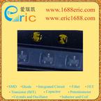
2SK2035 N沟道MOSFET 20V 100mA/0.1A SOT-523/SSM marking/标记 KP 高速开关/高输入阻抗/低栅极阈值电压
Pictures:
3D模型
符号图
焊盘图
引脚图
产品图
页面导航:
标记信息在P1
技术参数、封装参数在P1
应用领域在P1P5
电气规格在P2
导航目录
2SK2035数据手册
Page:
of 5 Go
若手册格式错乱,请下载阅览PDF原文件
2SK2035
2007-11-01
1
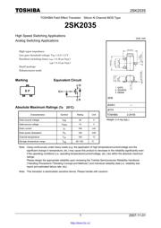
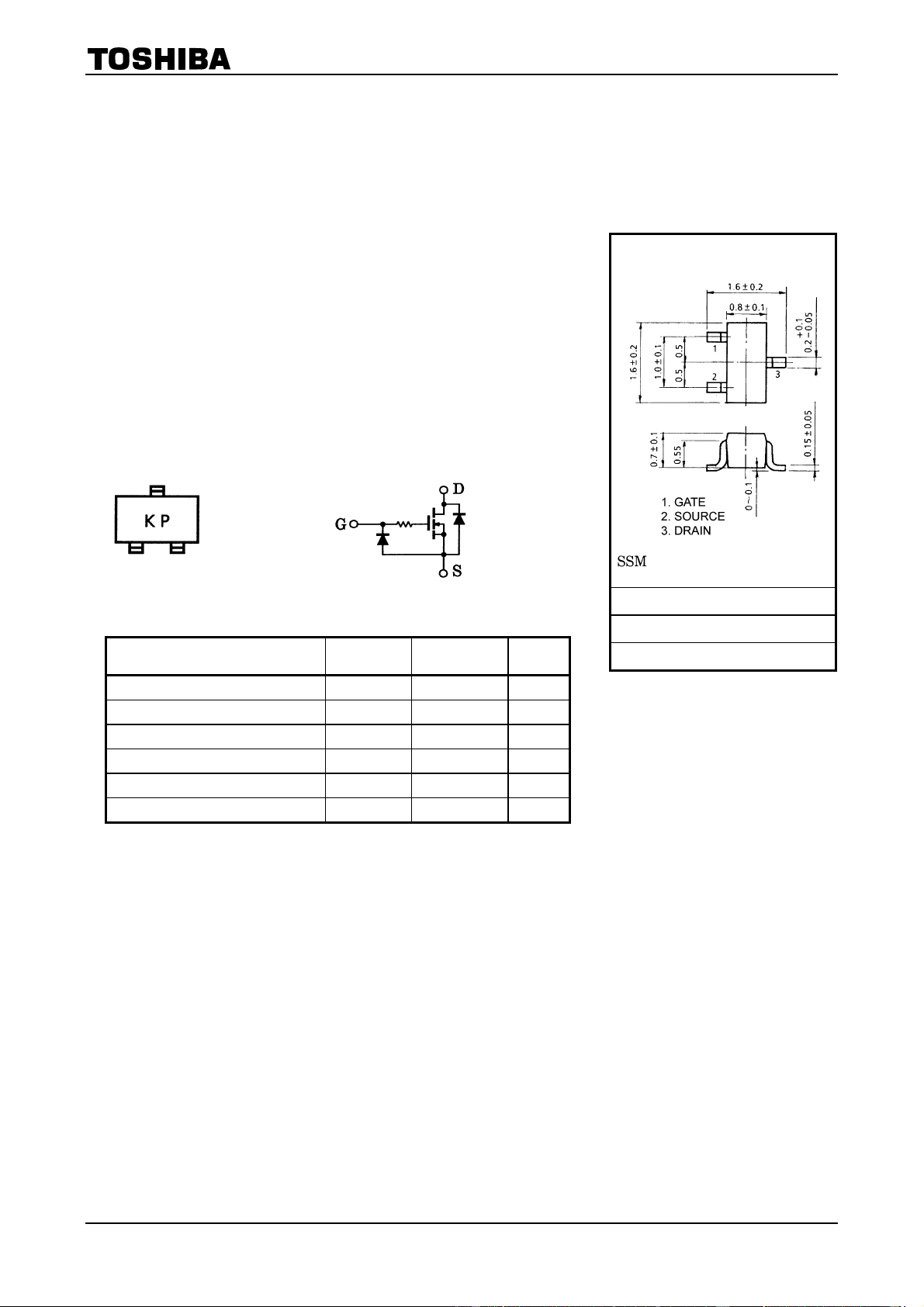
TOSHIBA Field Effect Transistor Silicon N Channel MOS Type
2SK2035
High Speed Switching Applications
Analog Switching Applications
High input impedance.
Low gate threshold voltage: V
th
= 0.5~1.5 V
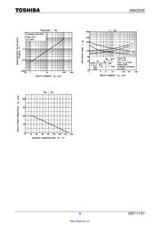
Excellent switching times: t
on
= 0.16 μs (typ.)
t
off
= 0.15 μs (typ.)
Small package
Enhancement-mode
Marking Equivalent Circuit
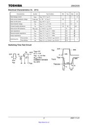
Absolute Maximum Ratings
(Ta 25°C)
Characteristics Symbol Rating Unit
Drain-source voltage V
DS
20 V
Gate-source voltage V
GSS
10 V
Drain current I
D
100 mA
Drain power dissipation P
D
100 mW
Channel temperature T
ch
150 °C
Storage temperature range T
stg
55~150 °C
Note: Using continuously under heavy loads (e.g. the application of high temperature/current/voltage and the
significant change in temperature, etc.) may cause this product to decrease in the reliability significantly even
if the operating conditions (i.e. operating temperature/current/voltage, etc.) are within the absolute maximum
ratings.
Please design the appropriate reliability upon reviewing the Toshiba Semiconductor Reliability Handbook
(“Handling Precautions”/“Derating Concept and Methods”) and individual reliability data (i.e. reliability test
report and estimated failure rate, etc).
Note: This transistor is electrostatic sensitive device. Please handle with caushon.
Unit: mm
JEDEC ―
JEITA ―
TOSHIBA 2-2H1B
Weight: 2.4 mg (typ.)
http://store.iiic.cc/
器件 Datasheet 文档搜索
AiEMA 数据库涵盖高达 72,405,303 个元件的数据手册,每天更新 5,000 多个 PDF 文件
