Datasheet 搜索 > 逻辑芯片 > TI(德州仪器) > 74LVC161284DLRG4 数据手册 > 74LVC161284DLRG4 其他数据使用手册 1/11 页

 器件3D模型
¥ 0.806
74LVC161284DLRG4 其他数据使用手册 - TI(德州仪器)
制造商:
TI(德州仪器)
分类:
逻辑芯片
封装:
SSOP-48
描述:
19位总线接口 19-BIT BUS INTERFACE
Pictures:
3D模型
符号图
焊盘图
引脚图
产品图
页面导航:
导航目录
74LVC161284DLRG4数据手册
Page:
of 11 Go
若手册格式错乱,请下载阅览PDF原文件

74LVC374A
Document number: DS35895 Rev. 1 - 2
1 of 10
www.diodes.com
June 2014
© Diodes Incorporated
74LVC374A
NEW PRODUCT
OCTAL D-TYPE FLIP-FLOP WITH 3 STATE OUTPUTS
Description
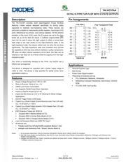
The 74LVC374A provides eight edge-triggered D-type flip-flops
featuring 3-state outputs designed specifically for driving highly
capacitive or relatively low-impedance loads. These devices are
particularly suitable for implementing buffer registers, input/output (I/O)
ports, bidirectional bus drivers, and working registers. On the positive
transition of the clock (CLK) input, the Q outputs are set to the logic
levels set up at the data (D) inputs. A buffered output-enable (OE)
input can be used to place the eight outputs in either a normal logic
state (high or low logic levels) or the high-impedance state. In the
high-impedance state, the outputs neither load nor drive the bus lines
significantly. The high-impedance state and increased drive provide
the capability to drive bus lines without interface or pullup components.
OE does not affect internal operations of the latch. Old data can be
retained or new data can be entered while the outputs are in the high-
impedance state.
The ‘374A is functionally identical to the ‘574A, but the’574 has a
different pin arrangement.
The device is designed for operation with a power supply range of
1.65V to 3.6V. The device is fully specified for partial power down
applications using I
OFF
.
Features
• Supply Voltage Range from 1.65V to 3.6V
• Sinks or Sources 24ma at V
CC
= 3V
• CMOS Low Power Consumption
• I
OFF
Supports Partial Power Down Operation
• Inputs or Outputs Accept Up to 5.5V
• Inputs Can Be Driven by 3.3V or 5V Allowing for Mixed Voltage
Applications
• Schmitt Trigger Action at All Inputs
• Typical V
OLP
(Quiet Output Ground Bounce) Less Than 0.8V with
V
CC
= 3.3V and T
A
= +25°C
• Typical V
OHV
(Quiet Output dynamic VOH) Greater than 2.0V with
V
CC
= 3.3V and T
A
= +25°C
• ESD Protection Tested per JESD 22
Exceeds 200-V Machine Model (A115)
Exceeds 2000-V Human Body Model (A114)
Exceeds 1000-V Charged Device Model (C101)
• Latch-Up Exceeds 250mA per JESD 78, Class I
• All devices are:
Totally Lead-Free & Fully RoHS compliant (Notes 1 & 2)
Halogen and Antimony Free. “Green” Device (Note 3)
Pin Assignments
1
3
2
4
5
6
7
8
Vcc
(Top View)
TSSOP-20
GND
10
9
13
14
12
11
17
18
16
15
19
20
2D
1D
2Q
3Q
3D
4D
4Q
1Q
OE
7Q
7D
6Q
6D
5D
5Q
CLK
8D
8Q
Top Transparent View
3
2
4
5
6
7
8
9
13
14
12
17
18
16
15
19
11 20
110
Vcc
8Q
7Q
7D
6Q
6D
5D
5Q
CLK
8D
GND
OE
2D
1D
2Q
3Q
3D
4D
4Q
1Q
QFN-20
(
)
terminal 1
index area
Applications
• General Purpose Logic
• Bus Driving
• Power Down Signal Isolation
• Wide array of products such as:
PCs, Notebooks, Netbooks, Ultrabooks
Networking Computer Peripherals, Hard Drives, CD/DVD
ROM
TV, DVD, DVR, Set Top Box
Notes: 1. No purposely added lead. Fully EU Directive 2002/95/EC (RoHS) & 2011/65/EU (RoHS 2) compliant.
2. See http://www.diodes.com/quality/lead_free.html for more information about Diodes Incorporated’s definitions of Halogen and Antimony free,
"Green" and Lead-Free.
3. Halogen and Antimony free "Green” products are defined as those which contain <900ppm bromine, <900ppm chlorine (<1500ppm total Br + Cl) and
<1000ppm antimony compounds.
器件 Datasheet 文档搜索
AiEMA 数据库涵盖高达 72,405,303 个元件的数据手册,每天更新 5,000 多个 PDF 文件
