Datasheet 搜索 > AD转换器 > ADI(亚德诺) > AD7715ARZ-5REEL 数据手册 > AD7715ARZ-5REEL 其他数据使用手册 5/40 页
 器件3D模型
¥ 43.403
AD7715ARZ-5REEL 其他数据使用手册 - ADI(亚德诺)
制造商:
ADI(亚德诺)
分类:
AD转换器
封装:
SOIC-16
描述:
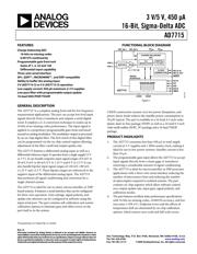
3 V / 5 V , 450 MUA 16位Σ-Δ型ADC 3 V/5 V, 450 muA 16-Bit, Sigma-Delta ADC
Pictures:
3D模型
符号图
焊盘图
引脚图
产品图
页面导航:
导航目录
AD7715ARZ-5REEL数据手册
Page:
of 40 Go
若手册格式错乱,请下载阅览PDF原文件
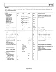
AD7715
Rev. D | Page 5 of 40
AD7715-3
AV
DD
= 3 V, DV
DD
= 3 V, REF IN (+) = 1.25 V; REF IN(−) = AGND; f
CLK IN
= 2.4576 MHz, unless otherwise noted. All specifications T
MIN
to T
MAX
, unless otherwise noted.
Table 2.
Parameter
1
Min Typ Max Unit Conditions/Comments
STATIC PERFORMANCE
No Missing Codes 16 Bits Guaranteed by design; filter notch ≤ 60 Hz
Output Noise See Table 18 to Table 22 Depends on filter cutoffs and selected gain
Integral Nonlinearity ±0.0015 % of FSR Filter notch ≤ 60 Hz
Unipolar Offset Error
2
See Table 15 to Table 22
Unipolar Offset Drift
3
0.2 μV/°C
Bipolar Zero Error
2
See Table 15 to Table 22
Bipolar Zero Drift
3
0.2 μV/°C
Positive Full-Scale Error
2, 4
See Table 15 to Table 22
Full-Scale Drift
3, 5
0.2 μV/°C
Gain Error
2, 6
See Table 15 to Table 22
Gain Drift
3, 7
0.2 ppm of
FSR/°C
Bipolar Negative Full-Scale Error
2
±0.003 % of FSR Typically ±0.0004%
Bipolar Negative Full-Scale Drift
3
1 μV/°C For gains of 1 and 2
0.6 μV/°C For gains of 32 and 128
ANALOG INPUTS/REFERENCE INPUTS Specifications for AIN and REF IN unless noted
Input Common-Mode Rejection
(CMR)
90 dB At dc; tpically 102 dB
Normal-Mode 50 Hz Rejection
8
98 dB For filter notches of 25 Hz, 50 Hz, ±0.02 × f
NOTCH
Normal-Mode 60 Hz Rejection
8
98 dB For filter notches of 20 Hz, 60 Hz, ±0.02 × f
NOTCH
Common-Mode 50 Hz Rejection
8
150 dB For filter notches of 25 Hz, 50 Hz, ±0.02 × f
NOTCH
Common-Mode 60 Hz Rejection
8
150 dB For filter notches of 20 Hz, 60 Hz, ±0.02 × f
NOTCH
Common-Mode Voltage Range
9
AGND AV
DD
V AIN for BUF bit of setup register = 0 and REF IN
Absolute AIN/REF IN Voltage
8
AGND − 0.03 AV
DD
+ 0.03 V AIN for BUF bit of setup register = 0 and REF IN
Absolute/Common-Mode AIN
Voltage
9
AGND + 0.05 AV
DD
− 1.5 V BUF bit of setup register = 1
AIN DC Input Current
8
1 nA
AIN Sampling Capacitance
8
10 pF
AIN Differential Voltage Range
10
0 to
+V
REF
/GAIN
11
nom
Unipolar input range (
B/U bit of setup register = 1)
±V
REF
/GAIN nom
Bipolar input range (
B/U bit of setup register = 0)
AIN Input Sampling Rate, f
S
GAIN × f
CLK IN
/64 For gains of 1 and 2
f
CLK IN
/8 For gains of 32 and 128
REF IN(+) − REF IN(−) Voltage 1.25 V nom ±1% for specified performance; functional with
lower V
REF
REF IN Input Sampling Rate, f
S
f
CLK IN
/64
LOGIC INPUTS
Input Current ±10 μA
All Inputs Except MCLK IN
V
INL
, Input Low Voltage 0.8 V
V
INH
, Input High Voltage 2.0 V
MCLK IN Only
V
INL
, Input Low Voltage 0.4 V
V
INH
, Input High Voltage 2.5 V
器件 Datasheet 文档搜索
AiEMA 数据库涵盖高达 72,405,303 个元件的数据手册,每天更新 5,000 多个 PDF 文件
