Datasheet 搜索 > AD转换器 > National Semiconductor(美国国家半导体) > ADC12062BIVF 数据手册 > ADC12062BIVF 其他数据使用手册 4/21 页


¥ 0
ADC12062BIVF 其他数据使用手册 - National Semiconductor(美国国家半导体)
制造商:
National Semiconductor(美国国家半导体)
分类:
AD转换器
描述:
12位, 1兆赫, 75毫瓦的A / D转换器 12-Bit, 1 MHz, 75 mW A/D Converter
Pictures:
3D模型
符号图
焊盘图
引脚图
产品图


ADC12062BIVF数据手册
Page:
of 21 Go
若手册格式错乱,请下载阅览PDF原文件
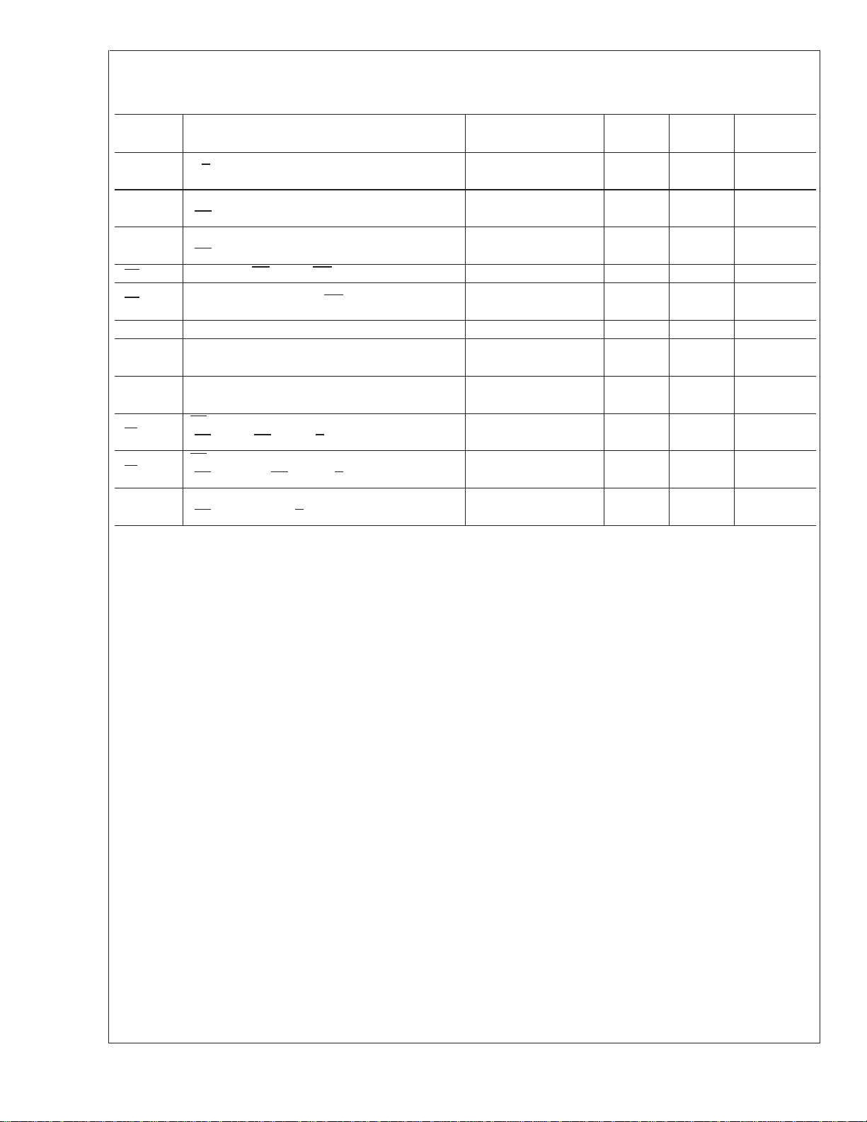
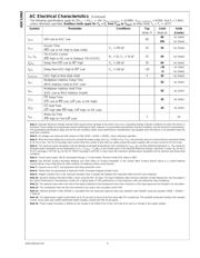
AC Electrical Characteristics (Continued)
The following specifications apply for DV
CC
=AV
CC
= +5V, V
REF+(SENSE)
= +4.096V, V
REF−(SENSE)
= AGND, and f
s
= 1 MHz,
unless otherwise specified. Boldface limits apply for T
A
=T
J
from T
MIN
to T
MAX
; all other limits T
A
=T
J
= +25˚C.
Symbol Parameter Conditions Typ Limit Units
(Note 7) (Note 8) (Limits)
t
EOC
S/H Low to EOC Low 95
60 ns (min)
185 ns (max)
t
ACC
Access Time
C
L
= 100 pF 10 20 ns (max)
(RD Low or OE High to Data Valid)
t
1H
,t
0H
TRI-STATE Control
R
L
= 1k, C
L
=10pF 25 40 ns (max)
(RD High or OE Low to Databus TRI-STATE)
t
INTH
Delay from RD Low to INT High C
L
= 100 pF 35 60 ns (max)
t
INTL
Delay from EOC High to INT Low C
L
= 100 pF −25
−35 ns (min)
−5 ns (max)
t
UPDATE
EOC High to New Data Valid 5 30 ns (max)
t
MS
Multiplexer Address Setup Time
50 ns (min)
(MUX Address Valid to EOC Low)
t
MH
Multiplexer Address Hold Time
50 ns (min)
(EOC Low to MUX Address Invalid)
t
CSS
CS Setup Time
20 ns (min)
(CS Low to RD Low, S/H Low, or OE High)
t
CSH
CS Hold Time
20 ns (min)
(CS High after RD High, S/H High, or OE Low)
t
WU
Wake-Up Time
1µs
(PD High to First S/H Low)
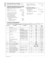
Note 1: Absolute Maximum Ratings indicate limits beyond which damage to the device may occur. Operating Ratings indicate conditions for which the device is
functional. These ratingsdo not guaranteespecific performance limits,however. For guaranteed specifications and test conditions, see the Electrical Characteristics.
The guaranteed specifications apply only for the test conditions listed. Some performance characteristics may degrade when the device is not operated under the
listed test conditions.
Note 2: All voltages are measured with respect to GND (GND = AGND = DGND), unless otherwise specified.
Note 3: When the input voltage (V
IN
) at any pin exceeds the power supply rails (V
IN
<
GND or V
IN
>
V
CC
) the absolute value of current at that pin should be limited
to 25 mA or less. The 50 mA package input current limits the number of pins that can safely exceed the power supplies with an input current of 25 mA to two.
Note 4: The maximum power dissipation must be derated at elevated temperatures and is dictated by T
JMAX
, θ
JA
and the ambient temperature T
A
. The maximum
allowable power dissipation at any temperature is P
D
=(T
JMAX
−T
A
)/θ
JA
or the number given in the Absolute Maximum Ratings, whichever is lower. θ
JA
for the V
(PLCC) package is 55˚C/W. θ
JA
for the VF (PQFP) package is 62˚C/W. In most cases the maximum derated power dissipation will be reached only during fault
conditions.
Note 5: Human body model, 100 pF discharged through a 1.5 kΩ resistor. Machine model ESD rating is 200V.
Note 6: See AN-450 “Surface Mounting Methods and Their Effect on Product Reliability” or the section titled “Surface Mount” found in a current National
Semiconductor Linear Data Book for other methods of soldering surface mount devices.
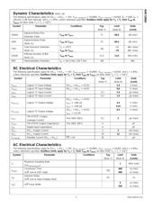
Note 7: Typicals are at +25˚C and represent most likely parametric norm.
Note 8: Tested limits are guaranteed to National’s AOQL (Average Outgoing Quality Level).
Note 9: Integral Linearity Error is the maximum deviation from a straight line between the measured offset and full scale endpoints.
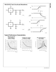
Note 10: Dynamic testing of the ADC12062 is done using the ADC IN input. The input multiplexer adds harmonic distortion at high frequencies. See the graph in
the Typical Performance Characteristics section for a typical graph of THD performance vs input frequency with and without the input multiplexer.
Note 11: The signal-to-noise ratio is the ratio of the signal amplitude to the background noise level. Harmonics of the input signal are not included in its calculation.
Note 12: The contributions from the first nine harmonics are used in the calculation of the THD.
Note 13: Effective Number of Bits (ENOB) is calculated from the measured signal-to-noise plus distortion ratio (SINAD) using the equation ENOB = (SINAD −
1.76)/6.02.
Note 14: The digital power supply current takes up to 10 seconds to decay to its final value after PD is pulled low. This prohibits production testing of the standby
current. Some parts may exhibit significantly higher standby currents than the 20 µA typical.
Note 15: Power Supply Sensitivity is defined as the change in the Offset Error or the Full Scale Error due to a change in the supply voltage.
ADC12062
www.national.com 4
器件 Datasheet 文档搜索
AiEMA 数据库涵盖高达 72,405,303 个元件的数据手册,每天更新 5,000 多个 PDF 文件
