Datasheet 搜索 > Flash芯片 > Cypress Semiconductor(赛普拉斯) > AM29F010B-90JF 数据手册 > AM29F010B-90JF 其他数据使用手册 5/33 页

¥ 7.595
AM29F010B-90JF 其他数据使用手册 - Cypress Semiconductor(赛普拉斯)
制造商:
Cypress Semiconductor(赛普拉斯)
分类:
Flash芯片
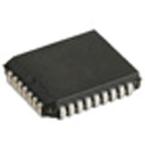
封装:
PLCC
Pictures:
3D模型
符号图
焊盘图
引脚图
产品图
页面导航:
导航目录
AM29F010B-90JF数据手册
Page:
of 33 Go
若手册格式错乱,请下载阅览PDF原文件

March 2, 2006 Am29F010B_00_C8 Am29F010B 3
DATA SHEET
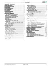
TABLE OF CONTENTS
General Description . . . . . . . . . . . . . . . . . . . . . . . . 2
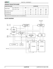
Product Selector Guide . . . . . . . . . . . . . . . . . . . . . 4
Block Diagram . . . . . . . . . . . . . . . . . . . . . . . . . . . . . 4
Connection Diagrams . . . . . . . . . . . . . . . . . . . . . . . 5
Pin Configuration . . . . . . . . . . . . . . . . . . . . . . . . . . 5
Logic Symbol . . . . . . . . . . . . . . . . . . . . . . . . . . . . . 5
Ordering Information . . . . . . . . . . . . . . . . . . . . . . . 6
Standard Products .................................................................... 6
Device Bus Operations . . . . . . . . . . . . . . . . . . . . . . 7
Table 1. Am29F010B Device Bus Operations .................................7
Requirements for Reading Array Data ..................................... 7
Writing Commands/Command Sequences .............................. 7
Program and Erase Operation Status ...................................... 8
Standby Mode .......................................................................... 8
Output Disable Mode ................................................................ 8
Table 2. Am29F010B Sector Addresses Table .................................8
Autoselect Mode ....................................................................... 8
Table 3. Am29F010B Autoselect Codes (High Voltage Method) ......9
Sector Protection/Unprotection ................................................. 9
Hardware Data Protection ........................................................ 9
Command Definitions . . . . . . . . . . . . . . . . . . . . . . 10
Reading Array Data ................................................................ 10
Reset Command ..................................................................... 10
Autoselect Command Sequence ............................................ 10
Byte Program Command Sequence ....................................... 10
Figure 1. Program Operation ..........................................................11
Chip Erase Command Sequence ........................................... 11
Sector Erase Command Sequence ........................................ 11
Erase Suspend/Erase Resume Commands ........................... 12
Figure 2. Erase Operation ...............................................................12
Table 4. Am29F010B Command Definitions ...................................13
Write Operation Status . . . . . . . . . . . . . . . . . . . . . 14
DQ7: Data# Polling ................................................................. 14
Figure 3. Data# Polling Algorithm ...................................................14
DQ6: Toggle Bit I .................................................................... 14
Reading Toggle Bit DQ6 ......................................................... 15
Figure 4. Toggle Bit Algorithm ........................................................ 15
DQ5: Exceeded Timing Limits ................................................ 15
DQ3: Sector Erase Timer ....................................................... 16
Table 5. Write Operation Status ..................................................... 16
Absolute Maximum Ratings . . . . . . . . . . . . . . . . 17
Figure 5. Maximum Negative Overshoot Waveform ...................... 17
Figure 6. Maximum Positive Overshoot Waveform ........................ 17
Operating Ranges . . . . . . . . . . . . . . . . . . . . . . . . 17
DC Characteristics . . . . . . . . . . . . . . . . . . . . . . . . 18
Test Conditions . . . . . . . . . . . . . . . . . . . . . . . . . . 20
Figure 7. Test Setup ....................................................................... 20
Table 6. Test Specifications ........................................................... 20
Key to Switching Waveforms . . . . . . . . . . . . . . . 20
AC Characteristics . . . . . . . . . . . . . . . . . . . . . . . . 21
Figure 8. Read Operations Timings ............................................... 21
Erase and Program Operations .............................................. 22
Figure 9. Program Operation Timings ............................................ 23
Figure 10. Chip/Sector Erase Operation Timings .......................... 23
Figure 11. Data# Polling Timings (During Embedded Algorithms) . 24
Figure 12. Toggle Bit Timings (During Embedded Algorithms) ...... 24
Erase and Program Operations .............................................. 25
Figure 13. Alternate CE# Controlled Write Operation Timings ...... 26
Erase and Programming Performance . . . . . . . 26
Latchup Characteristic . . . . . . . . . . . . . . . . . . . . 27
TSOP Pin Capacitance . . . . . . . . . . . . . . . . . . . . 27
PLCC and PDIP Pin Capacitance . . . . . . . . . . . . 27
Data Retention . . . . . . . . . . . . . . . . . . . . . . . . . . . 27
Physical Dimensions . . . . . . . . . . . . . . . . . . . . . . 28
PD 032—32-Pin Plastic DIP ................................................... 28
PL 032—32-Pin Plastic Leaded Chip Carrier ......................... 29
TS 032—32-Pin Standard Thin Small Outline Package ......... 30
Revision Summary . . . . . . . . . . . . . . . . . . . . . . . . 31
器件 Datasheet 文档搜索
AiEMA 数据库涵盖高达 72,405,303 个元件的数据手册,每天更新 5,000 多个 PDF 文件
