Datasheet 搜索 > 锁存器 > Fairchild(飞兆/仙童) > CD4044BCN 数据手册 > CD4044BCN 其他数据使用手册 1/14 页

 器件3D模型
¥ 0
CD4044BCN 其他数据使用手册 - Fairchild(飞兆/仙童)
制造商:
Fairchild(飞兆/仙童)
分类:
锁存器
封装:
DIP-16
描述:
四三态或非R / S锁存器。四三态与非R / S锁存器 Quad 3-STATE NOR R/S Latches . Quad 3-STATE NAND R/S Latches
Pictures:
3D模型
符号图
焊盘图
引脚图
产品图
CD4044BCN数据手册
Page:
of 14 Go
若手册格式错乱,请下载阅览PDF原文件
October 1987
Revised January 1999
CD4046BC Micropower Phase-Locked Loop
© 1999 Fairchild Semiconductor Corporation DS005968.prf www.fairchildsemi.com
CD4046BC
Micropower Phase-Locked Loop
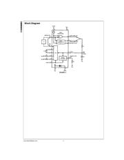
General Description
The CD4046BC micropower phase-locked loop (PLL) con-
sists of a low power, linear, voltage-controlled oscillator
(VCO), a source follower, a zener diode, and two phase
comparators. The two phase comparators have a common
signal input and a common comparator input. The signal
input can be directly coupled for a large voltage signal, or
capacitively coupled to the self-biasing amplifier at the sig-
nal input for a small voltage signal.
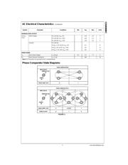
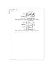
Phase comparator I, an exclusive OR gate, provides a digi-
tal error signal (phase comp. I Out) and maintains 90°
phase shifts at the VCO center frequency. Between signal
input and comparator input (both at 50% duty cycle), it may
lock onto the signal input frequencies that are close to har-
monics of the VCO center frequency.
Phase comparator II is an edge-controlled digital memory
network. It provides a digital error signal (phase comp. II
Out) and lock-in signal (phase pulses) to indicate a locked
condition and maintains a 0° phase shift between signal
input and comparator input.
The linear voltage-controlled oscillator (VCO) produces an
output signal (VCO Out) whose frequency is determined by
the voltage at the VCO
IN
input, and the capacitor and resis-
tors connected to pin C1
A
, C1
B
, R1 and R2.
The source follower output of the VCO
IN
(demodulator Out)
is used with an external resistor of 10 kΩ or more.
The INHIBIT input, when high, disables the VCO and
source follower to minimize standby power consumption.
The zener diode is provided for power supply regulation, if
necessary.
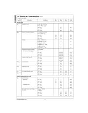
Features
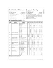
■ Wide supply voltage range: 3.0V to 18V
■ Low dynamic power consumption: 70 µW (typ.) at f
o
=
10 kHz, V
DD
= 5V
■ VCO frequency: 1.3 MHz (typ.) at V
DD
= 10V
■ Low frequency drift: 0.06%/°C at V
DD
= 10V with tem-
perature
■ High VCO linearity: 1% (typ.)
Applications
• FM demodulator and modulator
• Frequency synthesis and multiplication
• Frequency discrimination
• Data synchronization and conditioning
• Voltage-to-frequency conversion
• Tone decoding
• FSK modulation
• Motor speed control
Ordering Code:
Devices also available in Tape and Reel. Specify by appending the suffix letter “X” to the ordering code.
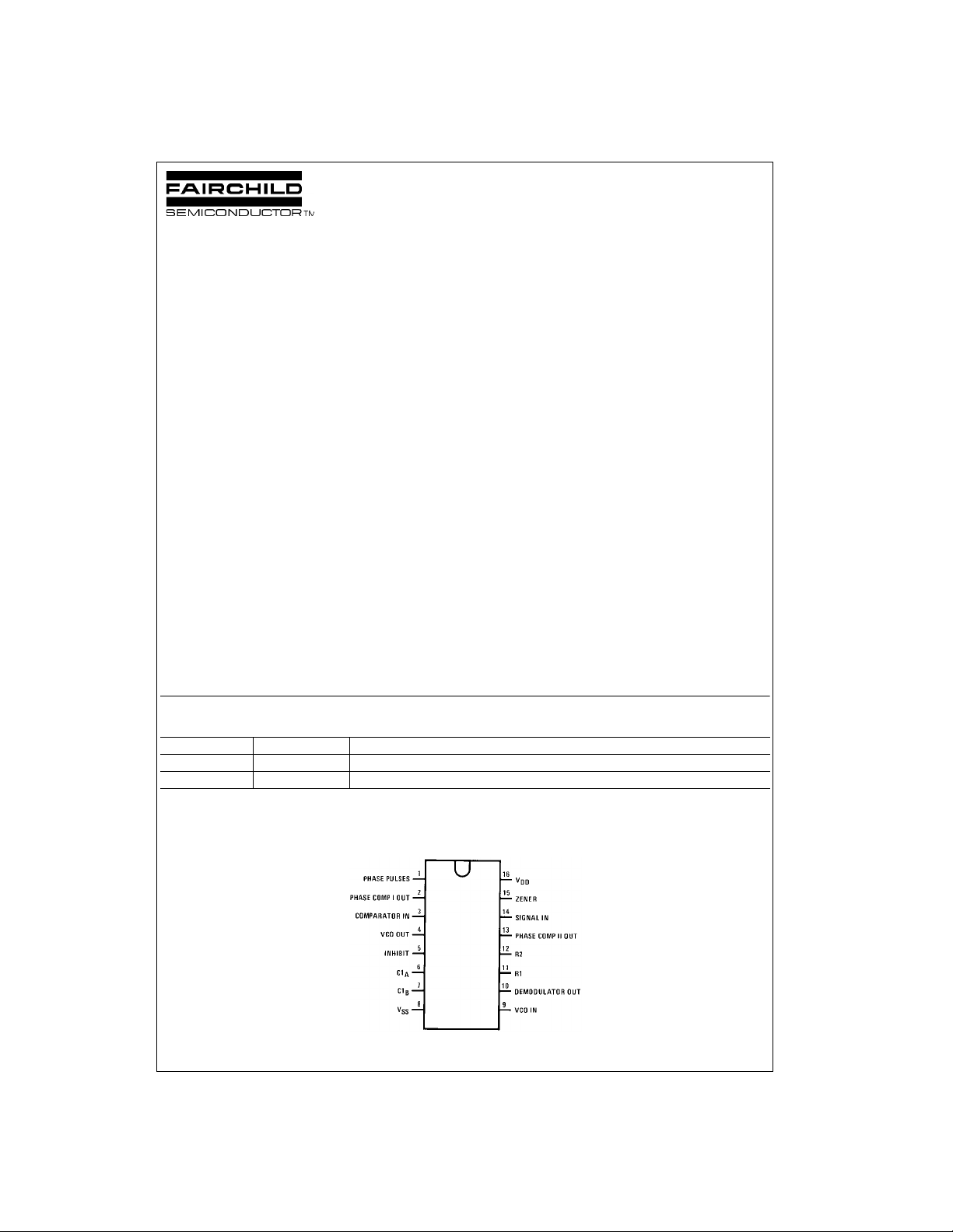
Connection Diagram
Pin Assignments for SOIC and DIP
Top View
Order Number Package Number Package Description
CD4046BCM M16A 16-Lead Small Outline integrated Circuit (SOIC), JEDEC MS-012, 0.150” Narrow Body
CD4046BCN N16E 16-Lead Plastic Dual-In-Line Package (PDIP), JEDEC MS-001, 0.300” Wide
器件 Datasheet 文档搜索
AiEMA 数据库涵盖高达 72,405,303 个元件的数据手册,每天更新 5,000 多个 PDF 文件
