Datasheet 搜索 > 接口芯片 > Maxim Integrated(美信) > DG508ADY+T 数据手册 > DG508ADY+T 其他数据使用手册 1/21 页
 器件3D模型
¥ 56.102
DG508ADY+T 其他数据使用手册 - Maxim Integrated(美信)
制造商:
Maxim Integrated(美信)
分类:
接口芯片
封装:
SOIC-16
描述:
模拟多路复用器/解复用器, 8:1, 1电路, 450 ohm, ±4.5V至±18V电源, NSOIC-16
Pictures:
3D模型
符号图
焊盘图
引脚图
产品图
页面导航:
导航目录
DG508ADY+T数据手册
Page:
of 21 Go
若手册格式错乱,请下载阅览PDF原文件

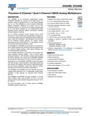
DG508B, DG509B
www.vishay.com
Vishay Siliconix
S14-2382-Rev. E, 15-Dec-14
1
Document Number: 64821
For technical questions, contact: analogswitchtechsupport@vishay.com
THIS DOCUMENT IS SUBJECT TO CHANGE WITHOUT NOTICE. THE PRODUCTS DESCRIBED HEREIN AND THIS DOCUMENT
ARE SUBJECT TO SPECIFIC DISCLAIMERS, SET FORTH AT www.vishay.com/doc?91000
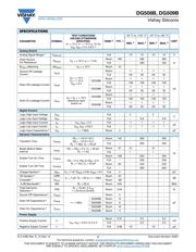
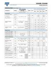
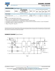
Precision 8-Channel / Dual 4-Channel CMOS Analog Multiplexers
DESCRIPTION
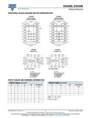
The DG508B is an 8-channel single-ended analog
multiplexer designed to connect one of eight inputs to a
common output as determined by a 3-bit binary address
(A
0
, A
1
, A
2
). The DG509B is a dual 4-channel differential
analog multiplexer designed to connect one of four
differential inputs to a common dual output as determined
by its 2-bit binary address (A
0
, A
1
). Break-before-make
switching action protects against momentary crosstalk
between adjacent channels.
An on channel conducts current equally well in both
directions. In the off state each channel blocks voltages up
to the power supply rails. An enable (EN) function allows the
user to reset the multiplexer / demultiplexer to all switches
off for stacking several devices. All control inputs,
addresses (A
X
) and enable (EN) are TTL compatible over the
full specified operating temperature range.
The DG508B and DG509B are fabricated on an enhanced
SG-II CMOS process that achieves improved performance
on: reduced charge injection, lower device leakage, and
minimized parasitic capacitance.
As the DG508, DG509 has a long history in the industry with
many suppliers offering copies - and in some cases
improved variations - with the best in class improvements,
the Vishay Siliconix new version of the DG508B, DG509B
are the superior alternatives to what is currently available.
Applications for the DG508B, DG509B include high speed
and high precision data acquisition, audio signal switching
and routing, ATE systems, and avionics. High performance
and low power dissipation make them ideal for battery
operated and remote instrumentation applications.
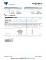
The DG508B and DG509B have the absolute maximum
voltage rating extended to 44 V. Additionally, single supply
operation is also allowed. An epitaxial layer prevents
latch-up.
The DG508B and DG509B are both available in 16-lead
SOIC, TSSOP, PDIP, and miniQFN (1.8 mm x 2.6 mm)
package options with extended temperature range of -40 °C
to +125 °C.
For more information, refer to Vishay Siliconix DG508B,
DG509B evaluation board note.
FEATURES
• Operate with single or dual power supply
• V+ to V- analog signal swing range
• 44 V power supply maximum rating
• Extended operate temperature range:
-40 °C to +125 °C
• Low leakage typically < 3 pA
• Low charge injection - Q
INJ
= 2 pC
• Low power - I
SUPPLY
: 10 μA
• TTL compatible logic
• > 250 mA latch-up current per JESD78
• Available in SOIC16, TSSOP16, PDIP, and miniQFN16
packages
• Superior alternative to:
- ADG508A, DG508A, HI-508
- ADG509A, DG509A, HI-509
• Material categorization: for definitions of compliance
please see www.vishay.com/doc?99912
BENEFITS
• Reduced switching errors
• Reduced glitching
• Improved data throughput
• Reduced power consumption
• Increased ruggedness
• Wide supply ranges (± 5 V to ± 20 V)
APPLICATIONS
• Data acquisition systems
• Audio and video signal routing
• ATE systems
• Medical instrumentation
器件 Datasheet 文档搜索
AiEMA 数据库涵盖高达 72,405,303 个元件的数据手册,每天更新 5,000 多个 PDF 文件
