Datasheet 搜索 > TVS二极管 > ON Semiconductor(安森美) > ESD7104MUTAG 数据手册 > ESD7104MUTAG 其他数据使用手册 1/12 页

¥ 1.406
ESD7104MUTAG 其他数据使用手册 - ON Semiconductor(安森美)
制造商:
ON Semiconductor(安森美)
分类:
TVS二极管
封装:
UDFN-10
描述:
ESD 保护阵列### 瞬态电压抑制器,On Semiconductor
Pictures:
3D模型
符号图
焊盘图
引脚图
产品图
页面导航:
引脚图在P1Hot
典型应用电路图在P1
原理图在P1P4
封装尺寸在P10P11
焊盘布局在P11
型号编码规则在P1P9P12
标记信息在P1P9P10P11P12
封装信息在P9
技术参数、封装参数在P9
应用领域在P1
电气规格在P2
型号编号列表在P1
导航目录
ESD7104MUTAG数据手册
Page:
of 12 Go
若手册格式错乱,请下载阅览PDF原文件
© Semiconductor Components Industries, LLC, 2016
July, 2020 − Rev. 6
1 Publication Order Number:
ESD7104/D
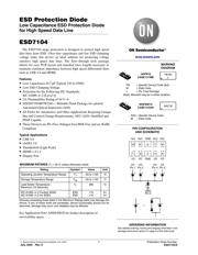
ESD Protection Diode
Low Capacitance ESD Protection Diode
for High Speed Data Line
ESD7104
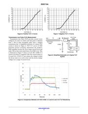
The ESD7104 surge protection is designed to protect high speed
data lines from ESD. Ultra−low capacitance and low ESD clamping
voltage make this device an ideal solution for protecting voltage
sensitive high speed data lines. The flow−through style package
allows for easy PCB layout and matched trace lengths necessary to
maintain consistent impedance between high speed differential lines
such as USB 3.0 and HDMI.
Features
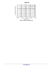
• Low Capacitance (0.3 pF Typical, I/O to GND)
• Low ESD Clamping Voltage
• Protection for the Following IEC Standards:
IEC 61000−4−2 (Level 4)
• UL Flammability Rating of 94 V−0
• SZESD7104MTWTAG − Wettable Flank Package for optimal
Automated Optical Inspection (AOI)
• SZ Prefix for Automotive and Other Applications Requiring Unique
Site and Control Change Requirements; AEC−Q101 Qualified and
PPAP Capable
• These Devices are Pb−Free, Halogen Free/BFR Free and are RoHS
Compliant
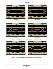
Typical Applications
• USB 3.0
• eSATA 3.0
• Thunderbolt (Light Peak)
• HDMI 1.3/1.4
• Display Port
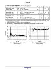
MAXIMUM RATINGS (T
J
= 25°C unless otherwise noted)
Rating
Symbol Value Unit
Operating Junction Temperature Range T
J
−55 to +125 °C
Storage Temperature Range T
stg
−55 to +150 °C
Lead Solder Temperature −
Maximum (10 Seconds)
T
L
260 °C
IEC 61000−4−2 Contact (ESD)
IEC 61000−4−2 Air (ESD)
ESD
ESD
±15
±15
kV
kV
Stresses exceeding those listed in the Maximum Ratings table may damage the
device. If any of these limits are exceeded, device functionality should not be
assumed, damage may occur and reliability may be affected.
See Application Note AND8308/D for further description of
survivability specs.
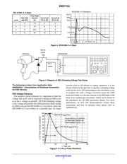
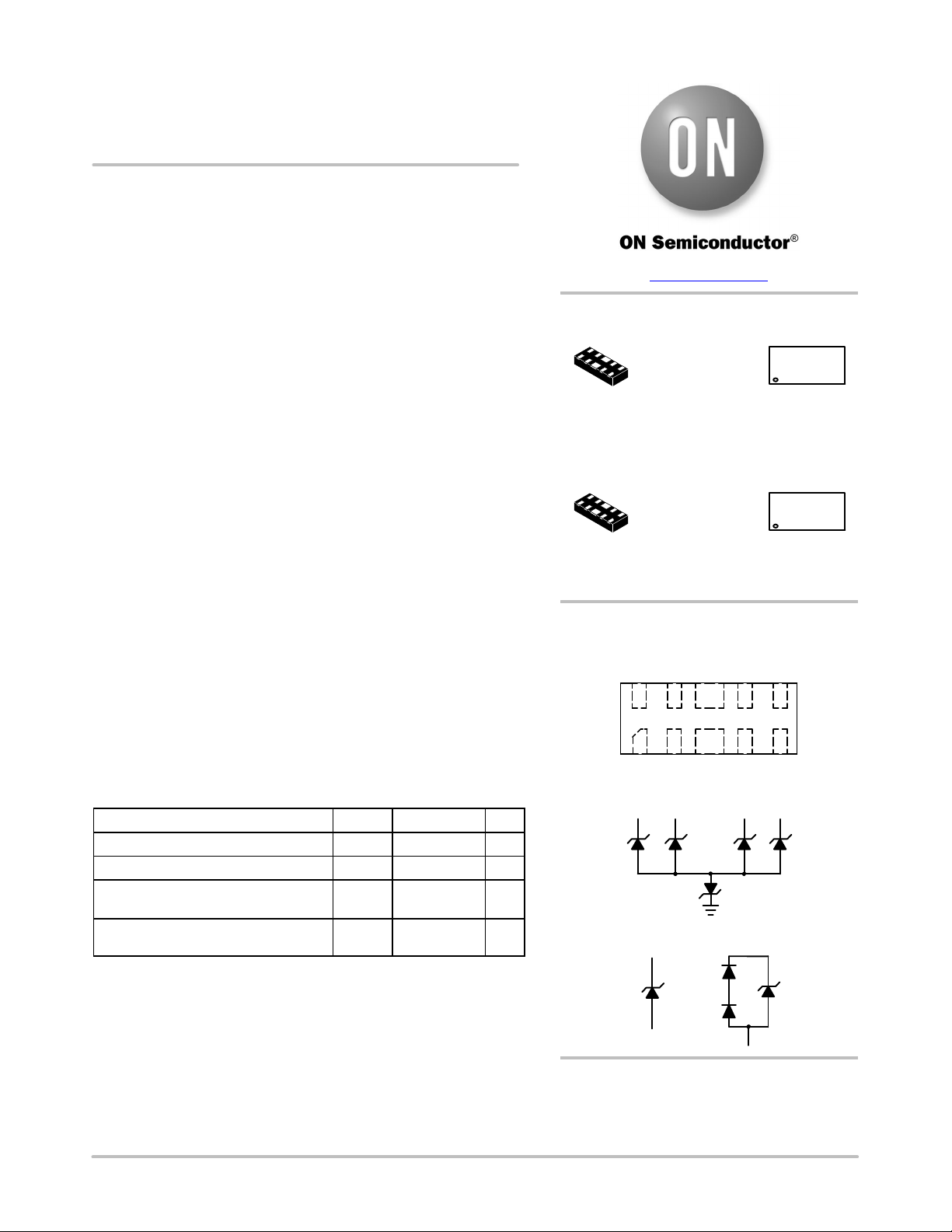
MARKING
DIAGRAM
UDFN10
CASE 517BB
PIN CONFIGURATION
AND SCHEMATIC
www.onsemi.com
7M MG
G
7M = Specific Device Code (tbd)
M = Date Code
G = Pb−Free Package
I/O I/O I/OI/O GND
N/C N/C N/C N/CGND
14523
10 7 698
(Note: Microdot may be in either location)
GND
Pin 2 Pin 4 Pin 5Pin 1
=
I/O I/O I/OI/O
Pin 3
See detailed ordering, marking and shipping information in the
package dimensions section on page 9 of this data sheet.
ORDERING INFORMATION
WDFNW10
CASE 515AH
AAC M
AAC = Specific Device Code
M = Date Code
器件 Datasheet 文档搜索
AiEMA 数据库涵盖高达 72,405,303 个元件的数据手册,每天更新 5,000 多个 PDF 文件
