Datasheet 搜索 > 收发器 > Finisar Corporation(菲尼萨) > FTLX3871DCC28 数据手册 > FTLX3871DCC28 产品描述及参数 3/13 页

¥ 6639.001
FTLX3871DCC28 产品描述及参数 - Finisar Corporation(菲尼萨)
制造商:
Finisar Corporation(菲尼萨)
分类:
收发器
描述:
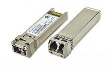
光纤发射器、接收器、收发器 15xxnm DWDM EML, APD , 8.5-11.3Gb/s trans
Pictures:
3D模型
符号图
焊盘图
引脚图
产品图
页面导航:
导航目录
FTLX3871DCC28数据手册
Page:
of 13 Go
若手册格式错乱,请下载阅览PDF原文件
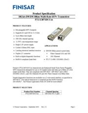
FTLX3871DCCxx Product Specification
Finisar Corporation – September 2015 Rev. C1 Page 3
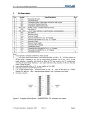
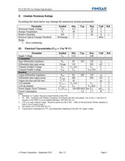
I. Pin Descriptions
Pin Symbol Name/Description Ref.
1 V
EET
Transmitter Ground 1
2 T
FAULT
Transmitter Fault 2
3 T
DIS
Transmitter Disable. Laser output disabled on high or open. 3
4 SDA 2-wire Serial Interface Data Line 2
5 SCL 2-wire Serial Interface Clock Line 2
6 MOD_ABS Module Absent. Grounded within the module 2
7 RS0 Rate Select 0. 4
8 RX_LOS Loss of Signal indication. Logic 0 indicates normal operation. 5
9 RS1
Rate Select 1. 4
10 V
EER
Receiver Ground 1
11 V
EER
Receiver Ground 1
12 RD-
Receiver Inverted DATA out. AC Coupled.
13 RD+ Receiver Non-inverted DATA out. AC Coupled.
14 V
EER
Receiver Ground 1
15 V
CCR
Receiver Power Supply 6
16 V
CCT
Transmitter Power Supply 6
17 V
EET
Transmitter Ground 1
18 TD+ Transmitter Non-Inverted DATA in. AC Coupled.
19 TD-
Transmitter Inverted DATA in. AC Coupled.
20 V
EET
Transmitter Ground 1
Notes:
1. Circuit ground is internally isolated from chassis ground.
2.
T
FAULT
is an open collector/drain output, which should be pulled up with a 4.7k – 10k Ohms resistor on
the host board if intended for use. Pull up voltage should be between 2.0V to Vcc + 0.3V. A high
output indicates a transmitter fault caused by either the TX bias current or the TX output power
exceeding the preset alarm thresholds. A low output indicates normal operation. In the low state, the
output is pulled to <0.8V.
3. Laser output disabled on T
DIS
>2.0V or open, enabled on T
DIS
<0.8V.
4. Internally pulled down per SFF-8431 Rev 4.1.
5. LOS is open collector output. Should be pulled up with 4.7k – 10k on host board to a voltage
between 2.0V and 3.6V. Logic 0 indicates normal operation; logic 1 indicates loss of signal.
6. Internally connected
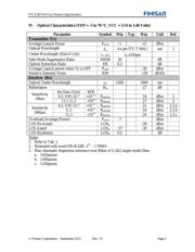
Figure 1. Diagram of Host Board Connector Block Pin Numbers and Names.
VeeT
VeeT
VeeR
VeeR
TD-
TD+
RD+
RD-
VccT
VccR
VeeT
VeeR
TX_Fault
SDA
SCL
MOD_ABS
RS0
RX_LOS
1
2
3
4
5
6
7
8
9
10
20
19
18
17
16
15
14
13
12
11
Towards
A
SIC
Towards
Bezel
TX_Disable
RS1
器件 Datasheet 文档搜索
AiEMA 数据库涵盖高达 72,405,303 个元件的数据手册,每天更新 5,000 多个 PDF 文件
