Datasheet 搜索 > Lattice Semiconductor(莱迪思) > GAL22V10C-10LJI 数据手册 > GAL22V10C-10LJI 其他数据使用手册 1/17 页


¥ 36.696
GAL22V10C-10LJI 其他数据使用手册 - Lattice Semiconductor(莱迪思)
制造商:
Lattice Semiconductor(莱迪思)
封装:
QCCJ
Pictures:
3D模型
符号图
焊盘图
引脚图
产品图
页面导航:
导航目录
GAL22V10C-10LJI数据手册
Page:
of 17 Go
若手册格式错乱,请下载阅览PDF原文件
GAL22LV10Z
GAL22LV10ZD
Low Voltage, Zero Power E
2
CMOS PLD
1
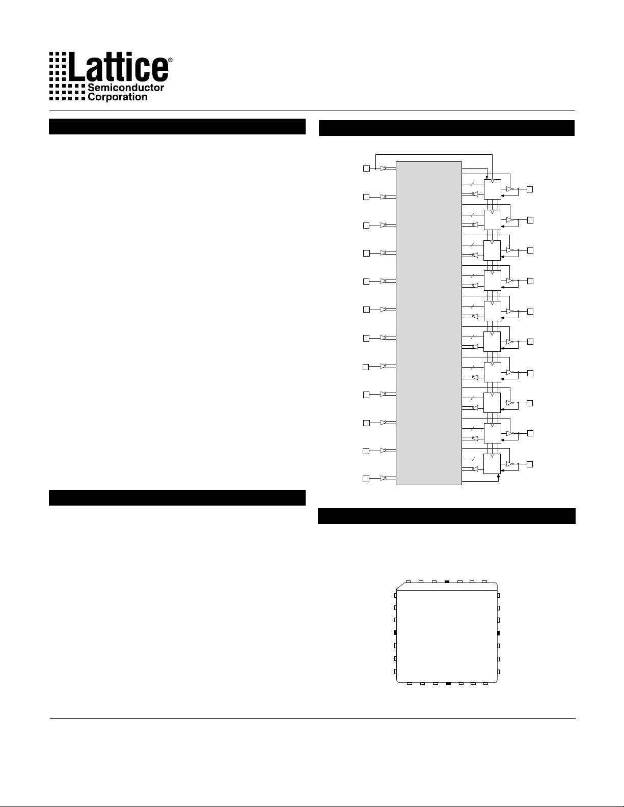
Description
The GAL22LV10Z and GAL22LV10ZD, at 15ns maximum propa-
gation delay time and 100µA standby current, combine 3.3V CMOS
process technology with Electrically Erasable (E
2
) floating gate tech-
nology to provide the best PLD solution to support today's new 3.3V
systems. E
2
technology offers high speed (<100ms) erase times,
providing the ability to reprogram or reconfigure the device quickly
and efficiently.
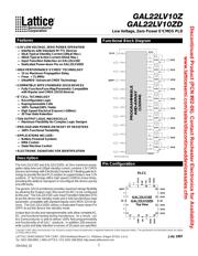
The generic 22V10 architecture provides maximum design flexibility
by allowing the Output Logic Macrocell (OLMC) to be configured
by the user. The GAL22LV10Z uses Input Transition Detection (ITD)
to put the device into standby mode and is fully function/fuse map/
parametric compatible with standard bipolar and CMOS 22V10 de-
vices. The GAL22LV10ZD utilizes a Dedicated Power-down Pin
(DPP) to put the device into standby mode.
Unique test circuitry and reprogrammable cells allow complete AC,
DC, and functional testing during manufacture. As a result, Lat-
tice Semiconductor is able to deliver 100% field programmability
and functionality of all GAL
®
products. In addition,100 erase/re-
write cycles and data retention in excess of 20 years are specified.
228
NC
I/CLK
I
I
I/DPP
I
I
I
I
I
NC
NC
NC
GND
I
I
I
I/O/Q
I/O/Q
I/O/Q
I/O/Q
I/O/Q
I/O/Q
I/O/Q
Vcc
I/O/Q
I/O/Q
I/O/Q
426
25
19
18
21
23
161412
11
9
7
5
PROGRAMMABLE
AND-ARRAY
(132X44)
I/O/Q
I/O/Q
I/O/Q
I/O/Q
I/O/Q
I/O/Q
I/O/Q
I/O/Q
I/O/Q
I/O/Q
*GAL22LV10ZD Only
I
I/CLK
I
I
I/DPP*
I
I
I
I
I
I
I
RESET
PRESET
8
10
12
14
16
16
14
12
10
8
OLMC
OLMC
OLMC
OLMC
OLMC
OLMC
OLMC
OLMC
OLMC
OLMC
PLCC
Copyright © 1997 Lattice Semiconductor Corp. All brand or product names are trademarks or registered trademarks of their respective holders. The specifications and information herein are subject
to change without notice.
LATTICE SEMICONDUCTOR CORP., 5555 Northeast Moore Ct., Hillsboro, Oregon 97124, U.S.A. July 1997
Tel. (503) 268-8000; 1-800-LATTICE; FAX (503) 268-8556; http://www.latticesemi.com
GAL22LV10Z
GAL22LV10ZD
Top View
22lv10zd_02
Features
• 3.3V LOW VOLTAGE, ZERO POWER OPERATION
— Interfaces with Standard 5V TTL Devices
—50
µA Typical Standby Current (100µA Max.)
— 40mA Typical Active Current (55mA Max.)
— Input Transition Detection on GAL22LV10Z
— Dedicated Power-down Pin on GAL22LV10ZD
• HIGH PERFORMANCE E
2
CMOS
®
TECHNOLOGY
— 15 ns Maximum Propagation Delay
— Fmax = 71.4MHz
— UltraMOS
®
Advanced CMOS Technology
• COMPATIBLE WITH STANDARD 22V10 DEVICES
— Fully Function/Fuse-Map/Parametric Compatible
with Bipolar and CMOS 22V10 Devices
•E
2
CELL TECHNOLOGY
— Reconfigurable Logic
— Reprogrammable Cells
— 100% Tested/100% Yields
— High Speed Electrical Erasure (<100ms)
— 20 Year Data Retention
• TEN OUTPUT LOGIC MACROCELLS
— Maximum Flexibility for Complex Logic Designs
• PRELOAD AND POWER-ON RESET OF REGISTERS
— 100% Functional Testability
• APPLICATIONS INCLUDE:
— Battery Powered Systems
— DMA Control
— State Machine Control
• ELECTRONIC SIGNATURE FOR IDENTIFICATION
Functional Block Diagram
Pin Configuration
Discontinued Product (PCN #02-06). Contact Rochester Electronics for Availability.
www.latticesemi.com/sales/discontinueddevicessales.cfm
器件 Datasheet 文档搜索
AiEMA 数据库涵盖高达 72,405,303 个元件的数据手册,每天更新 5,000 多个 PDF 文件
