Datasheet 搜索 > CPLD芯片 > Lattice Semiconductor(莱迪思) > GAL22V10D-15LJN 数据手册 > GAL22V10D-15LJN 产品设计图 1/124 页
 器件3D模型
¥ 31.042
GAL22V10D-15LJN 产品设计图 - Lattice Semiconductor(莱迪思)
制造商:
Lattice Semiconductor(莱迪思)
分类:
CPLD芯片
封装:
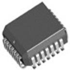
PLCC-28
描述:
SPLD - 简单可编程逻辑器件 HI PERF E2CMOS PLD
Pictures:
3D模型
符号图
焊盘图
引脚图
产品图
页面导航:
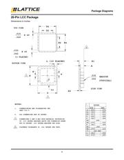
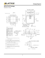
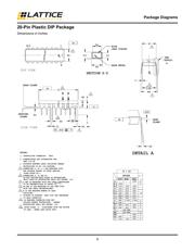
封装尺寸在P3P4P5P6P9P12P13P14P15P23P24P31
标记信息在P25P26P27P28P39P54P55P61P68P70P122
导航目录
GAL22V10D-15LJN数据手册
Page:
of 124 Go
若手册格式错乱,请下载阅览PDF原文件
www.latticesemi.com 1 pkg_5.2
Package Diagrams
June 2016 Data Sheet
© 2016 Lattice Semiconductor Corp. All Lattice trademarks, registered trademarks, patents, and disclaimers are as listed at www.latticesemi.com/legal. All other brand
or product names are trademarks or registered trademarks of their respective holders. The specifications and information herein are subject to change without notice.
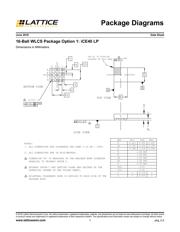
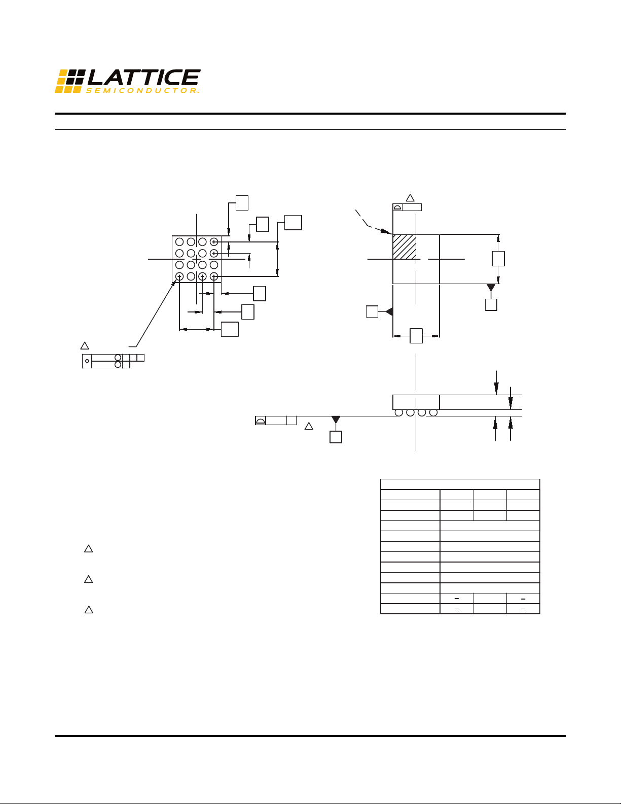
16-Ball WLCS Package Option 1: iCE40 LP
Dimensions in Millimeters
C
ccc
C
1
A
A
aaa
(4X)
.015
.05
B
M
M
C
C A
PIN #1 ID FIDUCIAL
LOCATED IN THIS AREA
REF.
Min. Nom. Max.
A
A1
b
D
E
D1
E1
e
aaa
ccc
r
s
0.413
0.122
0.188
0.452
0.152
0.218
0.491
0.182
0.248
1.40 BSC
1.48 BSC
1.05 BSC
1.05 BSC
0.35 BSC
0.03
0.03
0.175
0.215
4
E1
e
s
D1
e
r
A
B
C
D
3
.16 X b
Ø
Ø
Ø
5
E
B
A
D
ALL DIMENSIONS AND TOLERANCE PER ASME Y 14.5M - 1994.
ALL DIMENSIONS ARE IN MILLIMETERS.
DIMENSION “b” IS MEASURES AT THE MAXIMUM BUMP DIAMETER
PARALLEL TO PRIMARY DATUM C.
PRIMARY DATUM C AND SEATING PLANE ARE DEFINED BY THE
SPHERICAL CROWNS OF THE SOLDER BUMPS.
BILATERAL TOLERANCE ZONE IS APPLIED TO EACH SIDE OF THE
PACKAGE BODY.
NOTES:
3
4
5
1.
2.
4
3
2
1
TOP VIEW
BOTTOM VIEW
SIDE VIEW
器件 Datasheet 文档搜索
AiEMA 数据库涵盖高达 72,405,303 个元件的数据手册,每天更新 5,000 多个 PDF 文件
