Datasheet 搜索 > 放大器IC与RF模块 > Hittite > HMC613LC4B 数据手册 > HMC613LC4B 其他数据使用手册 1/11 页
 器件3D模型
¥ 7.264
HMC613LC4B 其他数据使用手册 - Hittite
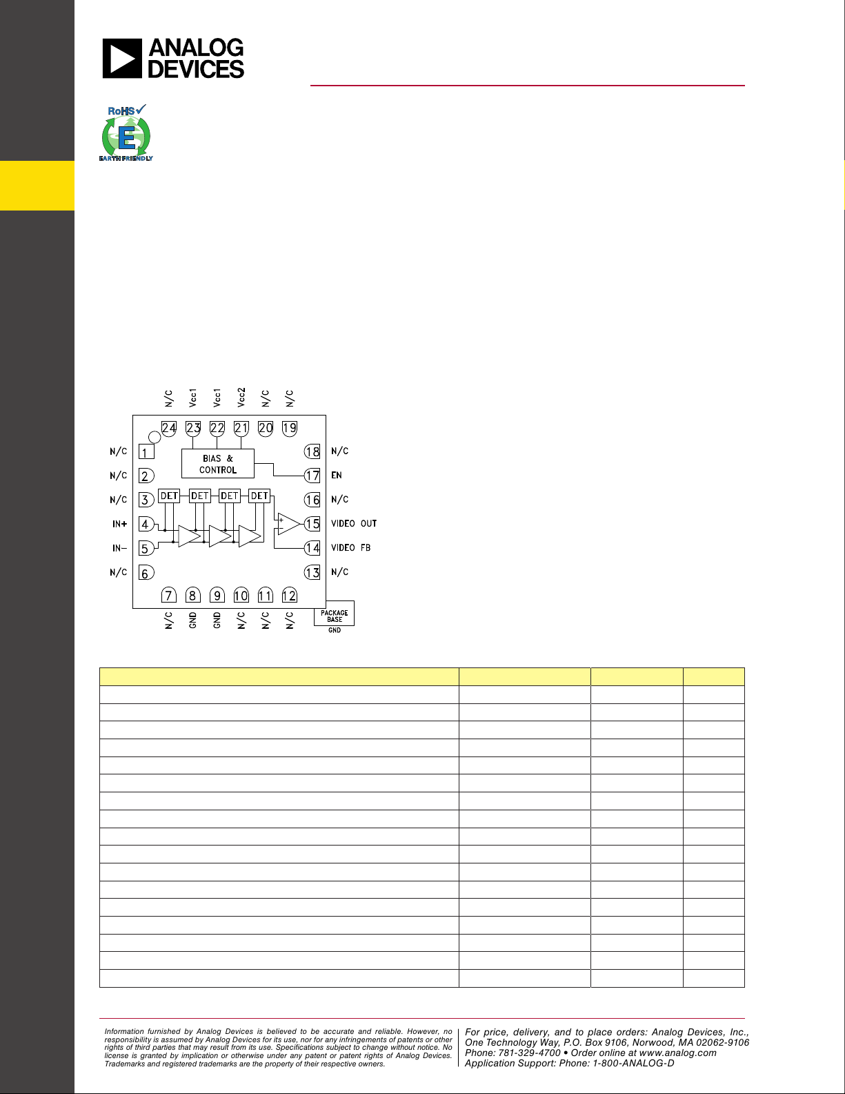
制造商:
Hittite
分类:
放大器IC与RF模块
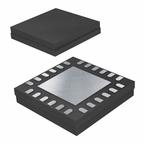
封装:
QFN-24
Pictures:
3D模型
符号图
焊盘图
引脚图
产品图
页面导航:
引脚图在P7P8Hot
典型应用电路图在P1
原理图在P7P8
封装尺寸在P6
标记信息在P6
封装信息在P1
功能描述在P1P7P8
技术参数、封装参数在P1P3P4P5P6P7P8P9P10P11
应用领域在P1
导航目录
HMC613LC4B数据手册
Page:
of 11 Go
若手册格式错乱,请下载阅览PDF原文件
For price, delivery and to place orders: Hittite Microwave Corporation, 2 Elizabeth Drive, Chelmsford, MA 01824
Phone: 978-250-3343 Fax: 978-250-3373 Order On-line at www.hittite.com
Application Support: Phone: 978-250-3343 or apps@hittite.com
POWER DETECTORS - SMT
1
HMC613LC4B
v11.0514
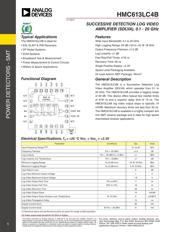
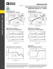
SUCCESSIVE DETECTION LOG VIDEO
AMPLIFIER (SDLVA), 0.1 - 20 GHz
The HMC613LC4B is a Successive Detection Log
Video Amplier (SDLVA) which operates from 0.1 to
20 GHz. The HMC613LC4B provides a logging range
of 59 dB. This device offers typical fast rise/fall times
of 4/18 ns and a superior delay time of 14 ns. The
HMC613LC4B log video output slope is typically 14
mV/dB. Maximum recovery times are less than 30 ns.
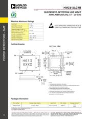
The HMC613LC4B is available in a highly compact 4x4
mm SMT ceramic package and is ideal for high speed
channelized receiver applications.
General Description
Features
Functional Diagram
Wide Input Bandwidth; 0.1 to 20 GHz
High Logging Range: 59 dB (-54 to +5) @ 18 GHz
Output Frequency Flatness: ±1.5 dB
Log Linearity: ±1 dB
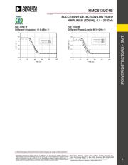
Fast Rise/Fall Times: 4/18 ns
Recovery Time: 26 ns
Single Positive Supply: +3.3V
Space Level Packaging Available
24 Lead 4x4mm SMT Package: 16mm
2
Typical Applications
The HMC613LC4B is ideal for:
• EW, ELINT & IFM Receivers
• DF Radar Systems
• ECM Systems
• Broadband Test & Measurement
• Power Measurement & Control Circuits
• Military & Space Applications
Electrical Specications, T
A
= +25 °C Vcc
1
= Vcc
2
= +3.3V
Parameter Conditions Typ. Units
Input Frequency Range
[1][2]
0.1 to 20 GHz
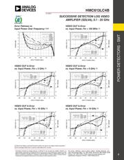
Frequency Flatness Pin = -25 dBm ±1.5 dB
Log Linearity Pin = -50 dBm to +3 dBm ±1 dBm
Log Linearity over Temperature Pin = -25dBm ±1 dB
Minimum Logging Range to ±3 dB error -54 @ 18 GHz dBm
Maximum Logging Range to ±3 dB error 5 @ 18 GHz dBm
Input Return Loss 8 dB
Log Video Minimum Output Voltage 1 V
Log Video Maximum Output Voltage 1.8 V
Log Video Output Rise Time 10% to 90% 4 ns
Log Video Output Fall Time 90% to 10% 18 ns
Log Video Recovery Time 26 ns
Log Video Output Slope 14 mV/dB
Log Video Output Slope Variation over Temperature @ 10 GHz 5 µV/dB°C
Log Video Propagation Delay 14 ns
Supply Current (Icc1) 80 mA
Supply Current (Icc2) @ Pin = -30 dBm 8 mA
[1] Electrical specs and performance plots are given for single-ended operation
[2] Video output load should be 1K Ohm or higher.
Information furnished by Analog Devices is believed to be accurate and reliable. However, no
responsibility is assumed by Analog Devices for its use, nor for any infringements of patents or other
rights of third parties that may result from its use. Specifications subject to change without notice. No
license is granted by implication or otherwise under any patent or patent rights of Analog Devices.
Trademarks and registered trademarks are the property of their respective owners.
For price, delivery, and to place orders: Analog Devices, Inc.,
One Technology Way, P.O. Box 9106, Norwood, MA 02062-9106
Phone: 781-329-4700 • Order online at www.analog.com
Application Support: Phone: 1-800-ANALOG-D
器件 Datasheet 文档搜索
AiEMA 数据库涵盖高达 72,405,303 个元件的数据手册,每天更新 5,000 多个 PDF 文件
