Datasheet 搜索 > 放大器IC与RF模块 > Hittite > HMC659LC5TR-R5 数据手册 > HMC659LC5TR-R5 其他数据使用手册 1/8 页

¥ 2307.532
HMC659LC5TR-R5 其他数据使用手册 - Hittite
制造商:
Hittite
分类:
放大器IC与RF模块
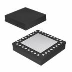
封装:
TFCQFN-32
Pictures:
3D模型
符号图
焊盘图
引脚图
产品图
页面导航:
导航目录
HMC659LC5TR-R5数据手册
Page:
of 8 Go
若手册格式错乱,请下载阅览PDF原文件
For price, delivery and to place orders: Hittite Microwave Corporation, 2 Elizabeth Drive, Chelmsford, MA 01824
Phone: 978-250-3343 Fax: 978-250-3373 Order On-line at www.hittite.com
Application Support: Phone: 978-250-3343 or apps@hittite.com
LINEAR & POWER AMPLIFIERS - SMT
1
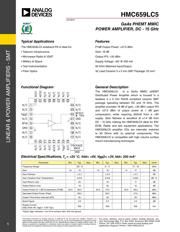
HMC659LC5
v04.0614
GaAs PHEMT MMIC
POWER AMPLIFIER, DC - 15 GHz
General Description
Features
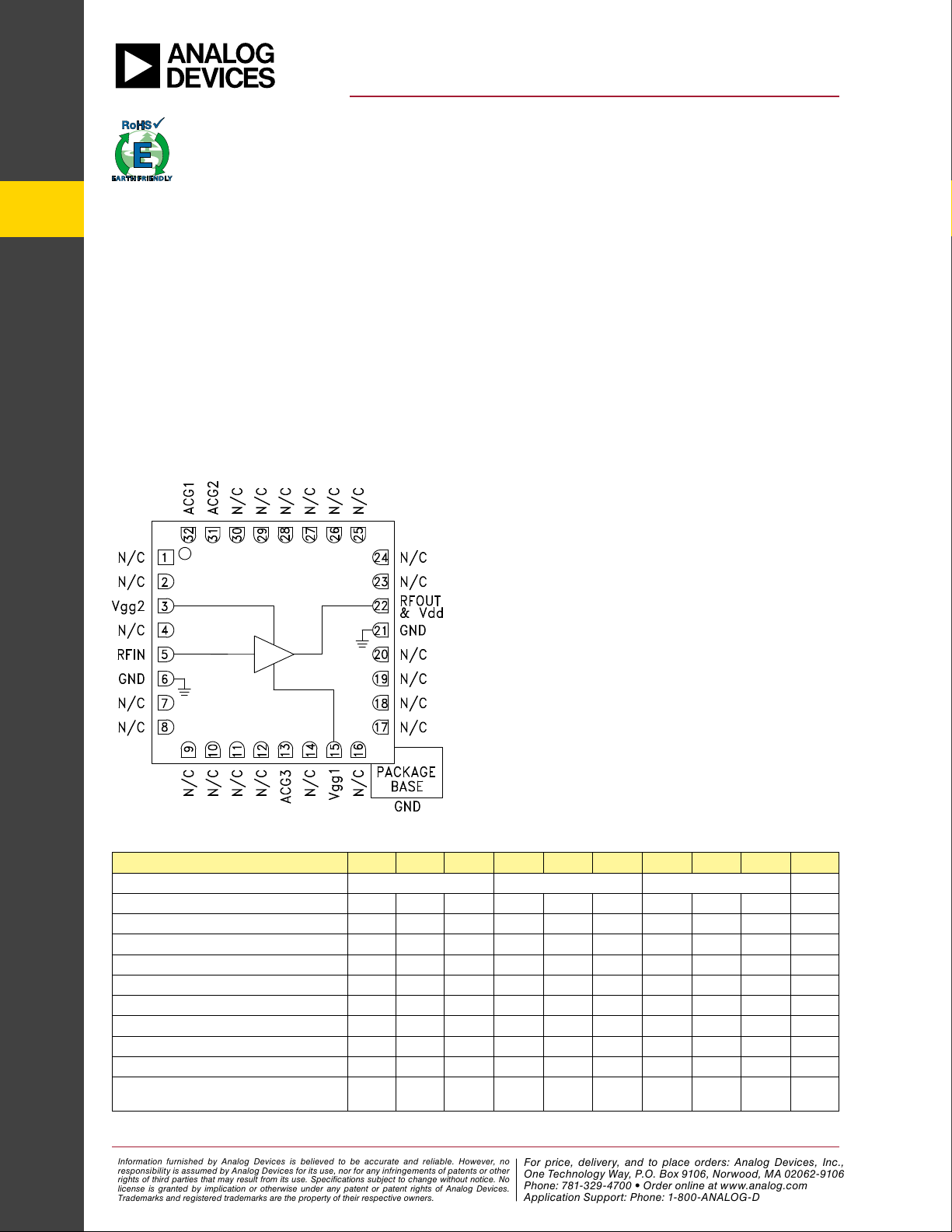
Functional Diagram
Typical Applications
The HMC659LC5 is a GaAs MMIC pHEMT
Distributed Power Amplier which is housed in a
leadless 5 x 5 mm RoHS compliant ceramic SMT
package operating between DC and 15 GHz. The
amplier provides 19 dB of gain, +35 dBm output IP3
and +27.5 dBm of output power at 1 dB gain
compression, while requiring 300mA from a +8V
supply. Gain atness is excellent at ±1.4 dB from
DC - 15 GHz making the HMC659LC5 ideal for EW,
ECM, Radar and test equipment applications. The
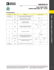
HMC659LC5 amplier I/Os are internally matched
to 50 Ohms with no external components. The
HMC659LC5 is compatible with high volume surface
mount manufacturing techniques.
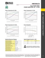
P1dB Output Power: +27.5 dBm
Gain: 19 dB
Output IP3: +35 dBm
Supply Voltage: +8V @ 300 mA
50 Ohm Matched Input/Output
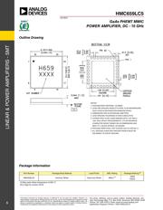
32 Lead Ceramic 5 x 5 mm SMT Package: 25 mm
2
The HMC659LC5 wideband PA is ideal for:
• Telecom Infrastructure
• Microwave Radio & VSAT
• Military & Space
• Test Instrumentation
• Fiber Optics
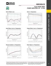
Electrical Specications, T
A
= +25 °C, Vdd= +8V, Vgg2= +3V, Idd= 300 mA*
Parameter Min. Typ. Max. Min. Typ. Max. Min. Typ. Max. Units
Frequency Range DC - 6 6 - 11 11 - 15 GHz
Gain 16 19 15 18 14 17 dB
Gain Flatness ± 0.7 ± 0.4 ± 0.7 dB
Gain Variation Over Temperature 0.015 0.019 0.022 dB/ °C
Input Return Loss 20 18 17 dB
Output Return Loss 19 20 15 dB
Output Power for 1 dB Compression (P1dB) 23.5 26.5 24.5 27.5 23.5 26.5 dBm
Saturated Output Power (Psat) 28.0 28.5 27.5 dBm
Output Third Order Intercept (IP3) 35 32 29 dBm
Noise Figure 3.0 2.5 3.5 dB
Supply Current
(Idd) (Vdd= 8V, Vgg1= -0.8V Typ.)
300 300 300 mA
*Adjust Vgg1 between -2 to 0V to achieve Idd= 300 mA typical.
Information furnished by Analog Devices is believed to be accurate and reliable. However, no
responsibility is assumed by Analog Devices for its use, nor for any infringements of patents or other
rights of third parties that may result from its use. Specifications subject to change without notice. No
license is granted by implication or otherwise under any patent or patent rights of Analog Devices.
Trademarks and registered trademarks are the property of their respective owners.
For price, delivery, and to place orders: Analog Devices, Inc.,
One Technology Way, P.O. Box 9106, Norwood, MA 02062-9106
Phone: 781-329-4700 • Order online at www.analog.com
Application Support: Phone: 1-800-ANALOG-D
器件 Datasheet 文档搜索
AiEMA 数据库涵盖高达 72,405,303 个元件的数据手册,每天更新 5,000 多个 PDF 文件
