Datasheet 搜索 > AD转换器 > ADI(亚德诺) > HMCAD1511 数据手册 > HMCAD1511 其他数据使用手册 6/32 页
 器件3D模型
¥ 479.985
HMCAD1511 其他数据使用手册 - ADI(亚德诺)
制造商:
ADI(亚德诺)
分类:
AD转换器
封装:
QFN-48
描述:
ANALOG DEVICES HMCAD1511 芯片, 高电涌保护器, 多模式, 8位, 1GSPS, 模数转换器
Pictures:
3D模型
符号图
焊盘图
引脚图
产品图
页面导航:
导航目录
HMCAD1511数据手册
Page:
of 32 Go
若手册格式错乱,请下载阅览PDF原文件
For price, delivery, and to place orders: Analog Devices, Inc., One Technology Way, P.O. Box 9106, Norwood,
MA 02062-9106
Phone: 781-329-4700 • Order online at www.analog.com
Application Support: Phone: 1-800-ANALOG-D
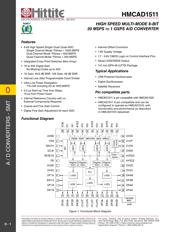
A / D CONVERTERS - SMT
0
0 - 4
HMCAD1511
v
04.1015
HIGH SPEED MULTI-MODE 8-BIT
30 MSPS to 1 GSPS A/D CONVERTER
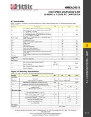
AC Specications
AVDD = 1.8V, DVDD = 1.8V, OVDD = 1.8V, 50% clock duty cycle, -1 dBFS 71 MHz input signal, Gain = 1X, RSDS output data levels unless
otherwise noted
Parameter Description Min Typ Max Unit
X
tlk,2
CrossTalk Dual Ch Mode. Signal applied to 1 channel (F
IN0
).
Measurement taken on one channel with full scale at F
IN1
.
F
IN1
= 71 MHz, F
IN0
= 70 MHz
65 dBc
X
tlk,4
CrossTalk Quad Ch Mode. Signal applied to 1 channel
(F
IN0
). Measurement taken on one channel with full scale at
F
IN1
. F
IN1
= 71 MHz, F
IN0
= 70 MHz
70 dBc
Power Supply
Single Ch: F
S
= 1 GSPS, Dual Ch: F
S
= 500 MSPS, Quad
Ch: F
S
= 250 MSPS.
I
AVDD
Analog Supply Current 270 mA
I
DVDD
Digital and output driver Supply Current 125 mA
P
AVDD
Analog Power 486 mW
P
DVDD
Digital Power 224 mW
P
TOT
Total Power Dissipation 710 mW
P
PD
Power Down Mode dissipation 15 µW
P
SLP
Deep sleep Mode power dissipation 72 mW
P
SLPCH
Power dissipation with all channels in sleep channel mode
(Light sleep)
153 mW
P
SLPCH_SAV
Power dissipation savings per channel off (Quad Channel
mode)
139 mW
Analog Input
FPBW Full Power Bandwidth 650 MHz
Clock Inputs
F
Smax
Max. Conversion Rate in Modes: Single Ch 1000 /
MSPS
Dual Ch / Quad Ch 500 / 250
F
smin
Min. Conversion Rate in Modes: Single Ch 120 /
MSPS
Dual Ch / Quad Ch 60 / 30
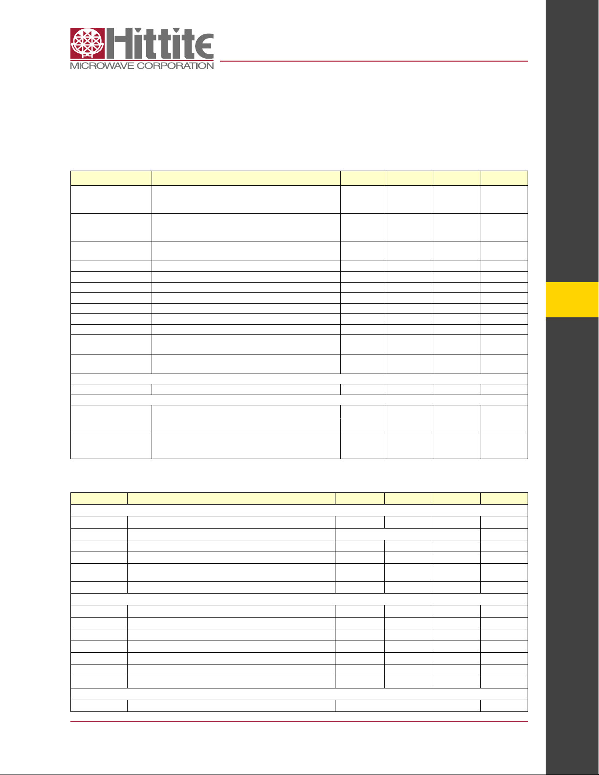
Digital and Switching Specications
AVDD = 1.8V, DVDD = 1.8V, OVDD = 1.8V, RSDS output data levels, unless otherwise noted
Parameter Description Min Typ Max Unit
Clock Inputs
DC Duty Cycle 45 55 % high
Compliance LVDS supported up to 700 MHz LVPECL, Sine wave, CMOS, LVDS
V
CK,sine
Differential input voltage swing, sine wave clock input 1500 mVpp
V
CK,CMOS
Voltage input range CMOS (CLKN connected to ground) V
OVDD
V
CM,CK
Input common mode voltage. Keep voltages within ground and
voltage of OVDD
0.3 V
OVDD
-0.3 V
C
CK
Differential Input capacitance 3 pF
Logic inputs (CMOS)
V
HI
High Level Input Voltage. V
OVDD
≥ 3.0V 2 V
V
HI
High Level Input Voltage. V
OVDD
= 1.7V – 3.0V 0.8 ·V
OVDD
V
V
LI
Low Level Input Voltage. V
OVDD
≥ 3.0V 0 0.8 V
V
LI
Low Level Input Voltage. V
OVDD
= 1.7V – 3.0V 0 0.2 ·V
OVDD
V
I
HI
High Level Input leakage Current +/-10 µA
I
LI
Low Level Input leakage Current +/-10 µA
C
I
Input Capacitance 3 pF
Data Outputs
Compliance LVDS / RSDS
器件 Datasheet 文档搜索
AiEMA 数据库涵盖高达 72,405,303 个元件的数据手册,每天更新 5,000 多个 PDF 文件
