Datasheet 搜索 > 稳压芯片 > TI(德州仪器) > LP5907SNX-1.8/NOPB 数据手册 > LP5907SNX-1.8/NOPB 产品封装文件 1/12 页

¥ 0.937
LP5907SNX-1.8/NOPB 产品封装文件 - TI(德州仪器)
制造商:
TI(德州仪器)
分类:
稳压芯片
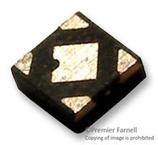
封装:
X2SON-4
描述:
TEXAS INSTRUMENTS LP5907SNX-1.8/NOPB 固定电压稳压器, LDO, 2.2V至5.5V, 120mV压差, 1.8V输出, 250mA输出, X2SON-4
Pictures:
3D模型
符号图
焊盘图
引脚图
产品图
页面导航:
导航目录
LP5907SNX-1.8/NOPB数据手册
Page:
of 12 Go
若手册格式错乱,请下载阅览PDF原文件
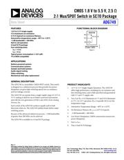
CMOS 1.8 V to 5.5 V, 2.5 Ω
2:1 Mux/SPDT Switch in SC70 Package
Data Sheet
ADG749
Rev. C
Information furnished by Analog Devices is believed to be accurate and reliable. However, no
responsibility is assumed by Analog Devices for its use, nor for any infringements of patents or other
rights of third parties that may result from its use. Specifications subject to change without notice. No
license is granted by implication or otherwise under any patent or patent rights of Analog Devices.
Trademarks and registered trademarks are the property of their respective owners.
One Technology Way, P.O. Box 9106, Norwood, MA 02062-9106, U.S.A.
Tel: 781.329.4700 www.analog.com
Fax: 781.461.3113 ©2001–2011 Analog Devices, Inc. All rights reserved.
FEATURES
1.8 V to 5.5 V single supply
5 Ω (maximum) on resistance
0.75 Ω (typical) on resistance flatness
Automotive temperature range: −40°C to +125°C
–3 dB bandwidth > 200 MHz
Rail-to-rail operation
6-lead SC70 package
Fast switching times
t
ON
= 12 ns
t
OFF
= 6 ns
Typical power consumption (< 0.01 μW)
TTL/CMOS compatible
APPLICATIONS
Battery-powered systems
Communication systems
Sample-and-hold systems
Audio signal routing
Video switching
Mechanical reed relay replacement
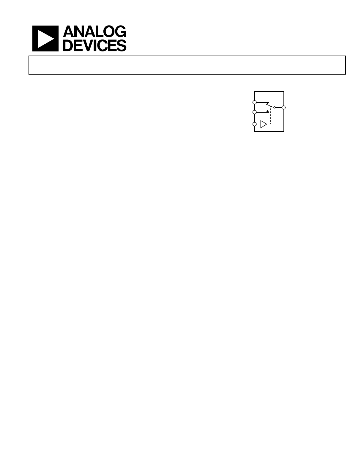
FUNCTIONAL BLOCK DIAGRAM
02075-001
SWITCH SHOWN FOR
A LOGIC 1 INPUT
ADG749
S2
S1
IN
D
Figure 1.
GENERAL DESCRIPTION
The ADG749 is a monolithic CMOS SPDT switch. This switch
is designed on a submicron process that provides low power
dissipation yet gives high switching speed, low on resistance,
and low leakage currents.
The ADG749 can operate from a single-supply range of 1.8 V to
5.5 V, making it ideal for use in battery-powered instruments
and with the new generation of DACs and ADCs from Analog
Devices, Inc.
Each switch of the ADG749 conducts equally well in both
directions when on. The ADG749 exhibits break-before-make
switching action.
Because of the advanced submicron process, −3 dB bandwidths
of greater than 200 MHz can be achieved.
The ADG749 is available in a 6-lead SC70 package.
PRODUCT HIGHLIGHTS
1. 1.8 V to 5.5 V Single-Supply Operation. The ADG749
offers high performance, including low on resistance and
fast switching times, and is fully specified and guaranteed
with 3 V and 5 V supply rails.
2. Ver y Low R
ON
(5 Ω Maximum at 5 V and 10 Ω Maximum
at 3 V). At 1.8 V operation, R
ON
is typically 40 Ω over the
temperature range.
3. Automotive Temperature Range: −40°C to +125°C.
4. On Resistance Flatness (R
FLAT(ON)
) (0.75 Ω typical).
5. −3 dB Bandwidth > 200 MHz.
6. Low Power Dissipation. CMOS construction ensures low
power dissipation.
7. Fast t
ON
/t
OFF
.
8. Tiny, 6-lead SC70 Package.
器件 Datasheet 文档搜索
AiEMA 数据库涵盖高达 72,405,303 个元件的数据手册,每天更新 5,000 多个 PDF 文件
