Datasheet 搜索 > 双极性晶体管 > ON Semiconductor(安森美) > MJE18004 数据手册 > MJE18004 其他数据使用手册 1/11 页

¥ 0.952
MJE18004 其他数据使用手册 - ON Semiconductor(安森美)
制造商:
ON Semiconductor(安森美)
分类:
双极性晶体管
封装:
TO-220-3
描述:
功率晶体管 POWER TRANSISTOR
Pictures:
3D模型
符号图
焊盘图
引脚图
产品图
页面导航:
封装尺寸在P10
型号编码规则在P1P10
标记信息在P1
电气规格在P2P3
导航目录
MJE18004数据手册
Page:
of 11 Go
若手册格式错乱,请下载阅览PDF原文件
© Semiconductor Components Industries, LLC, 2010
April, 2010 − Rev. 6
1 Publication Order Number:
MJE18004D2/D
MJE18004D2G
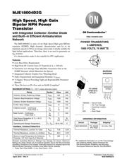
High Speed, High Gain
Bipolar NPN Power
Transistor
with Integrated Collector−Emitter Diode
and Built−in Efficient Antisaturation
Network
The MJE18004D2 is state−of−art High Speed High gain BIPolar
transistor (H2BIP). High dynamic characteristics and lot to lot
minimum spread (±150 ns on storage time) make it ideally suitable for
light ballast applications. Therefore, there is no need to guarantee an
h
FE
window.
It’s characteristics make it also suitable for PFC application.
Features
• Low Base Drive Requirement
• High Peak DC Current Gain (55 Typical) @ I
C
= 100 mA
• Extremely Low Storage Time Min/Max Guarantees Due to the
H2BIP Structure which Minimizes the Spread
• Integrated Collector−Emitter Free Wheeling Diode
• Fully Characterized and Guaranteed Dynamic V
CE(sat)
• “6 Sigma” Process Providing Tight and Reproductible Parameter
Spreads
• These Devices are Pb−Free and are RoHS Compliant*
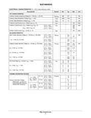
MAXIMUM RATINGS (T
J
= 25°C unless otherwise noted)
Rating Symbol Value Unit
Collector−Emitter Sustaining Voltage V
CEO
450 Vdc
Collector−Base Breakdown Voltage V
CBO
1000 Vdc
Collector−Emitter Breakdown Voltage V
CES
1000 Vdc
Emitter−Base Voltage V
EBO
12 Vdc
Collector Current − Continuous
Collector Current − Peak (Note 1)
I
C
I
CM
5
10
Adc
Base Current − Continuous
Base Current − Peak (Note 1)
I
B
I
BM
2
4
Adc
Total Device Dissipation @ T
C
= 25_C
Derate above 25°C
P
D
75
0.6
W
W/°C
Operating and Storage Temperature T
J
, T
stg
–65 to 150 °C
THERMAL CHARACTERISTICS
Thermal Resistance, Junction−to−Case
R
q
JC
1.65
_C/W
Thermal Resistance, Junction−to−Ambient
R
q
JA
62.5
_C/W
Maximum Lead Temperature for Soldering
Purposes: 1/8″ from Case for 5 Seconds
T
L
260
_C
Stresses exceeding Maximum Ratings may damage the device. Maximum
Ratings are stress ratings only. Functional operation above the Recommended
Operating Conditions is not implied. Extended exposure to stresses above the
Recommended Operating Conditions may affect device reliability.
1. Pulse Test: Pulse Width = 5 ms, Duty Cycle ≤ 10%.
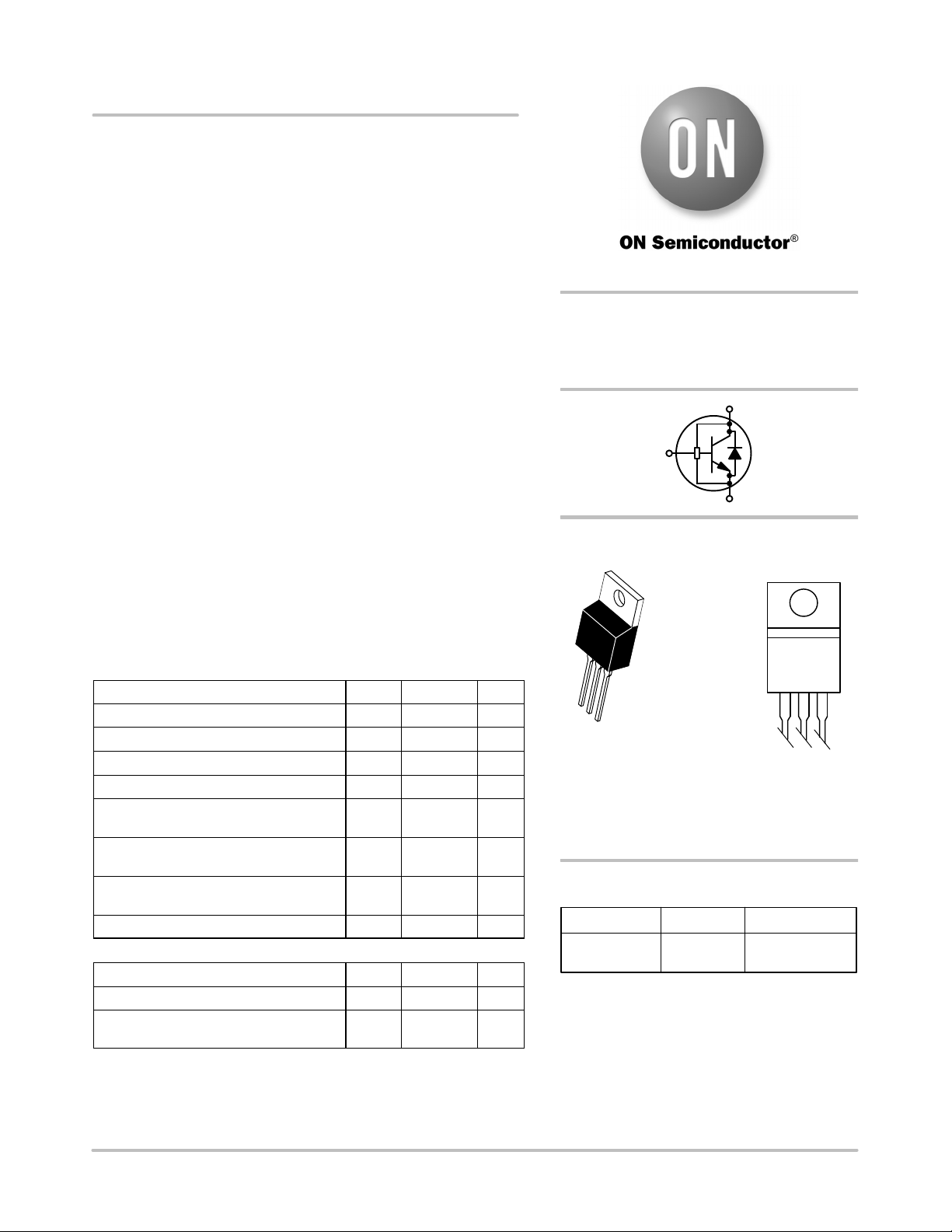
POWER TRANSISTORS
5 AMPERES,
1000 VOLTS, 75 WATTS
TO−220AB
CASE 221A
STYLE 1
1
2
3
4
http://onsemi.com
18004D2 = Device Code
G = Pb−Free Package
A = Assembly Location
Y = Year
WW = Work Week
MARKING
DIAGRAM
18004D2G
AYWW
Device Package Shipping
†
ORDERING INFORMATION
MJE18004D2G TO−220AB
(Pb−Free)
50 Units / Rail
*For additional information on our Pb−Free strategy
and soldering details, please download the
ON Semiconductor Soldering and Mounting
Techniques Reference Manual, SOLDERRM/D.
器件 Datasheet 文档搜索
AiEMA 数据库涵盖高达 72,405,303 个元件的数据手册,每天更新 5,000 多个 PDF 文件
