Datasheet 搜索 > TVS二极管 > ON Semiconductor(安森美) > MURS110T3G 数据手册 > MURS110T3G 产品修订记录 1/9 页

¥ 0.799
MURS110T3G 产品修订记录 - ON Semiconductor(安森美)
制造商:
ON Semiconductor(安森美)
分类:
TVS二极管
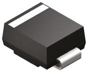
封装:
DO-214AA
描述:
2A 至 3A,ON Semiconductor### 标准带 NSV- 或 SUR- 前缀的制造商部件号符合 AEC-Q101 汽车等级。### 二极管和整流器,ON Semiconductor
Pictures:
3D模型
符号图
焊盘图
引脚图
产品图
页面导航:
标记信息在P1
封装信息在P1
导航目录
MURS110T3G数据手册
Page:
of 9 Go
若手册格式错乱,请下载阅览PDF原文件
TEM001790 Rev. B Page 1 of 4
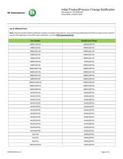
Initial Product/Process Change Notification
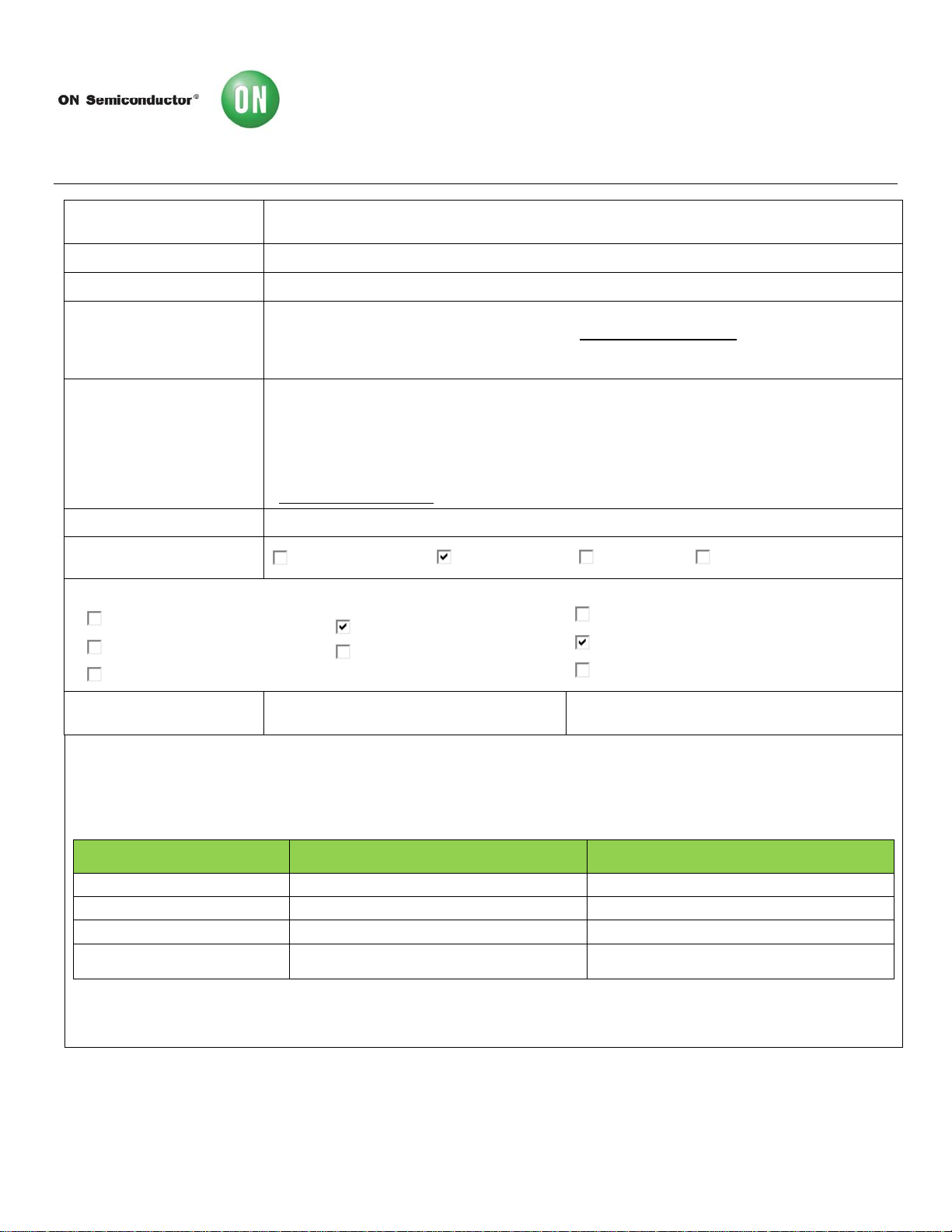
Document # : IPCN22541X
Issue Date: 22March2019
TitleofChange:
QualificationofHighDensityLeadframe from6rowsto16rowsandBOMChangeforSMBPackageinSub‐
ContractorFactorySeeful
ProposedFirstShipdate:
22September2019orearlieruponcustomerapproval
ContactInformation:
ContactyourlocalONSemiconductorSalesOfficeor<norsahida.sahman@onsemi.com>
Samples:
Samplesshouldbeavailableaftercompletionofqualification.
ContactyourlocalONSemiconductorSalesOfficeor<PCN.Samples@onsemi.com>
Samplerequestsaretobesubmittednolaterthan30daysfromthedateoffirstnotification,InitialPCNor
FinalPCN,forthischange.
TypeofNotification:
This is an Initial Product/Process Change Notification (IPCN) sent to customers. An IPCN is an advance
notificationaboutanupcomingchangeandcontainsgeneralinformationregardingthechangedetailsand
devicesaffected.Italsocontainsthepreliminaryreliabilityqualificationplan.
ThecompletedqualificationandcharacterizationdatawillbeincludedintheFinalProduct/ProcessChange
Notification (FPCN). ThisIPCN notificationwillbefollowed bya Final Product/Process Change Notification
(FPCN) at least 90 days prior to implementation of the change. In case of questions, contact
<PCN.Support@onsemi.com>
ChangePartIdentification:
Affectedproductswillbeidentifiedbydatecode.
ChangeCategory:
WaferFabChange
Assembl yChange TestChange Other
____________
ChangeSub‐Category(s):
ManufacturingSiteAddi tion
Manufacturi ngSite Transfer
Manufacturi ngProcessChange
MaterialChange
Productspecificchange
Datasheet/ProductDocchange
Shi pping/Packaging/Marking
Other:
__________________
SitesAffected:
ONSemiconductorSites:
None
ExternalFoundry/SubconSites:
ShanghaiSeeful
DescriptionandPurpose:
Thisis theinitial notificationannouncing that ONSemiconductor subcontractor factory(Shanghai Seeful) isqualifyinghigh density leadframe
from6‐rowsto16‐rowsincludingBOMchangeasshowninbelowtable.Earlystudyshowsdeviceperformanceandreliabilityisnoteffected.This
changewillallowOnSemiconductortomeetincreasingdemandforourSMBdeviceproducts.
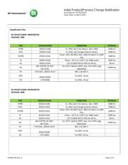
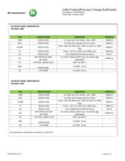
BeforeChangeDescription AfterChangeDescription
LeadFrame 6‐rowsleadframewithC194material 16‐rowsleadframewithC19210material
Clip 6‐rowsclip 16‐rowsclipanddesignchange
MoldCompound KL‐G100S EK1700GS
Carriertape Widertolerance
NewdesignbasedonJEDECspec,narrow
tolerancetoavoidpartmovingincarrierpocket
Thereisnoproductmarkingchangeasaresultofthischange.
器件 Datasheet 文档搜索
AiEMA 数据库涵盖高达 72,405,303 个元件的数据手册,每天更新 5,000 多个 PDF 文件
