Datasheet 搜索 > 模拟开关芯片 > ON Semiconductor(安森美) > NCV8452STT1G 数据手册 > NCV8452STT1G 其他数据使用手册 1/20 页

¥ 6.245
NCV8452STT1G 其他数据使用手册 - ON Semiconductor(安森美)
制造商:
ON Semiconductor(安森美)
分类:
模拟开关芯片
封装:
SOT-223-4
描述:
自我保护高边驱动器,带温度关断和电流限制
Pictures:
3D模型
符号图
焊盘图
引脚图
产品图
页面导航:
引脚图在P4Hot
典型应用电路图在P2
原理图在P2
封装尺寸在P19
焊盘布局在P18P19
型号编码规则在P1P18P19
标记信息在P1P19
封装信息在P18
焊接温度在P3
功能描述在P4
技术参数、封装参数在P18
应用领域在P1
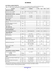
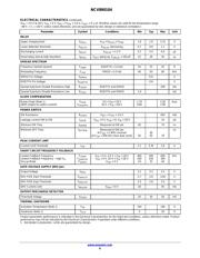
电气规格在P5P6
型号编号列表在P3
导航目录
NCV8452STT1G数据手册
Page:
of 20 Go
若手册格式错乱,请下载阅览PDF原文件

© Semiconductor Components Industries, LLC, 2015
August, 2017 − Rev. 4
1 Publication Order Number:
NCV890104/D
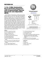
NCV890104
1.2 A, 2 MHz Automotive
Buck Switching Regulator
with Programmable Spread
Spectrum and Adjustable
RSTB
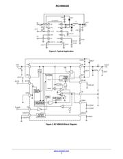
The NCV890104 is a fixed−frequency, monolithic, Buck switching
regulator intended for Automotive, battery−connected applications
that must operate with up to a 36 V input supply. The regulator is
suitable for systems with low noise and small form factor
requirements often encountered in automotive driver information
systems. The NCV890104 is capable of converting the typical 4.5 V to
18 V automotive input voltage range to outputs as low as 3.3 V at
a constant switching frequency above the sensitive AM band,
eliminating the need for costly filters and EMI countermeasures.
A Reset pin signals when the output is in regulation, and a pin is
provided to adjust the delay before the RSTB signal goes high.
The NCV890104 also provides several protection features expected in
Automotive power supply systems such as current limit, short circuit
protection, and thermal shutdown. In addition, the high switching
frequency produces low output voltage ripple even when using small
inductor values and an all−ceramic output filter capacitor − forming
a space−efficient switching regulator solution.
Features
• Internal N−Channel Power Switch
• Low V
IN
Operation Down to 4.5 V
• High V
IN
Operation to 36 V
• Withstands Load Dump to 40 V
• 2 MHz Free−running Switching Frequency
• Adjustable Spread Spectrum
• Reset with Adjustable Delay
• Logic level Enable Input Can be Directly Tied to
Battery
• 1.4 A (min) Cycle−by−Cycle Peak Current Limit
• Short Circuit Protection enhanced by Frequency
Foldback
• ±1.75% Output Voltage Tolerance
• Output Voltage Adjustable Down to 0.8 V
• 1.4 Millisecond Internal Soft−Start
• Thermal Shutdown (TSD)
• Low Shutdown Current
• NCV Prefix for Automotive and Other Applications
Requiring Unique Site and Control Change
Requirements; AEC−Q100 Qualified and PPAP
Capable
• Wettable Flanks DFN (pin edge plating)
• These Devices are Pb−Free and RoHS Compliant
Applications
• Audio
• Infotainment
• Safety − Vision Systems
• Instrumentation
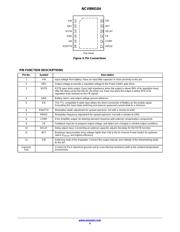
DFN12
CASE 506CE
MARKING DIAGRAM
A = Assembly Location
L = Wafer Lot
Y = Year
W = Work Week
G = Pb−Free Device
www.onsemi.com
(Note: Microdot may be in either location)
See detailed ordering and shipping information in the package
dimensions section on page 18 of this data sheet.
ORDERING INFORMATION
1
V8901
04
ALYWG
G
器件 Datasheet 文档搜索
AiEMA 数据库涵盖高达 72,405,303 个元件的数据手册,每天更新 5,000 多个 PDF 文件
