Datasheet 搜索 > 放大器、缓冲器 > ON Semiconductor(安森美) > NE5517NG 数据手册 > NE5517NG 其他数据使用手册 1/16 页
 器件3D模型
¥ 6.439
NE5517NG 其他数据使用手册 - ON Semiconductor(安森美)
制造商:
ON Semiconductor(安森美)
分类:
放大器、缓冲器
封装:
DIP-16
描述:
双通道互导放大器
Pictures:
3D模型
符号图
焊盘图
引脚图
产品图
页面导航:
引脚图在P1P2Hot
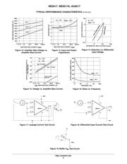
典型应用电路图在P7
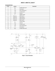
原理图在P2
封装尺寸在P14P15
焊盘布局在P14
型号编码规则在P1P13P15
标记信息在P1P15
封装信息在P13
技术参数、封装参数在P13
应用领域在P1P7P8
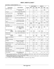
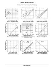
电气规格在P4P5P6
导航目录
NE5517NG数据手册
Page:
of 16 Go
若手册格式错乱,请下载阅览PDF原文件
© Semiconductor Components Industries, LLC, 2013
June, 2013 − Rev. 4
1 Publication Order Number:
NE5517/D
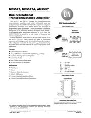
NE5517, NE5517A, AU5517
Dual Operational
Transconductance Amplifier
The AU5517 and NE5517 contain two current-controlled
transconductance amplifiers, each with a differential input and
push-pull output. The AU5517/NE5517 offers significant design and
performance advantages over similar devices for all types of
programmable gain applications. Circuit performance is enhanced
through the use of linearizing diodes at the inputs which enable a
10 dB signal-to-noise improvement referenced to 0.5% THD. The
AU5517/NE5517 is suited for a wide variety of industrial and
consumer applications.
Constant impedance of the buffers on the chip allow general use of
the AU5517/NE5517. These buffers are made of Darlington
transistors and a biasing network that virtually eliminate the change of
offset voltage due to a burst in the bias current I
ABC
, hence eliminating
the audible noise that could otherwise be heard in high quality audio
applications.
Features
• Constant Impedance Buffers
• DV
BE
of Buffer is Constant with Amplifier I
BIAS
Change
• Excellent Matching Between Amplifiers
• Linearizing Diodes
• High Output Signal-to-Noise Ratio
• Pb−Free Packages are Available*
Applications
• Multiplexers
• Timers
• Electronic Music Synthesizers
• Dolby® HX Systems
• Current-Controlled Amplifiers, Filters
• Current-Controlled Oscillators, Impedances
*For additional information on our Pb−Free strategy and soldering details, please
download the ON Semiconductor Soldering and Mounting Techniques
Reference Manual, SOLDERRM/D.
http://onsemi.com
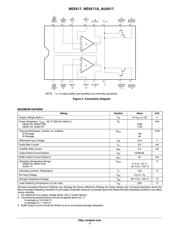
PIN CONNECTIONS
See detailed ordering and shipping information in the package
dimensions section on page 13 of this data sheet.
ORDERING INFORMATION
1
2
3
4
5
6
7
8
9
10
11
12
13
14
16
15
I
ABCa
D
a
+IN
a
−IN
a
VO
a
V−
IN
BUFFERa
VO
BUFFERa
I
ABCb
D
b
+IN
b
−IN
b
VO
b
V+
IN
BUFFERb
VO
BUFFERb
N, D Packages
(Top View)
PDIP−16
N SUFFIX
CASE 648
1
SOIC−16
D SUFFIX
CASE 751B
1
MARKING
DIAGRAMS
NE5517yy
AWLYYWWG
xx = AU or NE
yy = AN or N
A = Assembly Location
WL = Wafer Lot
YY, Y = Year
WW = Work Week
G = Pb−Free Package
xx5517DG
AWLYWW
1
1
器件 Datasheet 文档搜索
AiEMA 数据库涵盖高达 72,405,303 个元件的数据手册,每天更新 5,000 多个 PDF 文件
