Datasheet 搜索 > RF射频器件 > Nordic Semiconductor > NRF24LE1-F16Q32-T 数据手册 > NRF24LE1-F16Q32-T 其他数据使用手册 1/2 页
 器件3D模型
¥ 12.48
NRF24LE1-F16Q32-T 其他数据使用手册 - Nordic Semiconductor
制造商:
Nordic Semiconductor
分类:
RF射频器件
封装:
QFN-32
描述:
NRF24LE1 2.4GHz ISM 频段射频收发器 SoC**Nordic** **Semiconductor** **nRF24LE1** 是 2.4 GHz 收发器,带嵌入式微控制器,用于 ISM(工业、科学和医疗)无线电频段操作。 嵌入式基带协议引擎 (Enhanced ShockBurst™) 基于数据包通信,支持手动以及高级自主协议操作。nRF24L01+ 2.4GHz ISM 频段收发器 射频功率输出:高达 0dBm 接收器灵敏度:-94dBm @ 250kbps 调制:GFSK 最大 OTA 数据传输率:2Mbps 16MHz 8051 核心 MCU,具有 16KB 闪存,1KB RAM 和 1.5KB 限定的擦除/写入 NV 数据存储器 16-32 位乘/除协处理器 (MDU) AES 加密 HW 加速器 14 通道 6 到 12 位 ADC 多达 31 个 GPIO 串行输入/输出端口:SPI,I²C,UART 实时时钟 电源:+1.9 至 +3.6V 直流 应用:无线 PC 外设、运动手表和传感器、用于消费电子产品的射频远程控制、家庭和商用自动化、有源 RFID、资产跟踪系统、物联网 (IoT) 超低功率传感器网络 **RS 产品代码** 885-5757 7 x GPIO QFN24 885-5750 15 x GPIO QFN32 885-5754 31 x GPIO QFN48 ### 注NRF24L01+ RF 射频收发器核心作为单独的芯片供货。 (RS 885-5748)### 单芯片组件,Nordic Semiconductor展开
Pictures:
3D模型
符号图
焊盘图
引脚图
产品图
页面导航:
原理图在P1
功能描述在P1
技术参数、封装参数在P2
应用领域在P1P2
导航目录
NRF24LE1-F16Q32-T数据手册
Page:
of 2 Go
若手册格式错乱,请下载阅览PDF原文件
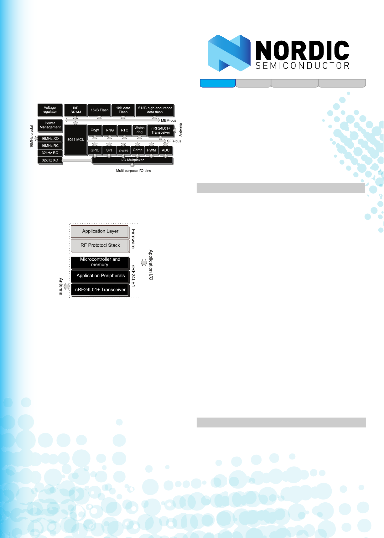
Single chip ultra low power wireless
Ultra low power wireless system-on-chip solution
The nRF24LE1 is a unique solution offering a complete ultra low power
(ULP) wireless system-on-chip (SoC) solution. It integrates the industry best
nRF24L01+ 2.4GHz transceiver core, an enhanced 8051 microcontroller,
ash memory and a wide range of analog and digital peripherals.
Block diagram
The 8-bit microcontroller is powerful enough to run both the RF protocol
stack and the application layer, enabling a true single chip implementation
of ULP wireless applications.
System diagram
Optimized for ultra low power wireless
Advanced power management and on-chip peripherals
The nRF24LE1 is optimized to provide a single chip solution for ULP
wireless applications. The combination of processing power, memory, low
power oscillators, real-time counter, AES encryption accelerator, random
generator, plus a range of power saving modes provides an ideal platform
for implementation of RF Protocols. Benets include tighter protocol timing,
security, lower power consumption and improved co-existence perform-
ance. For the application layer the nRF24LE1 offers a rich set of peripher-
als including: SPI, 2-wire, UART, 6 to 12-bit ADC, PWM, and an ultra low
power analog comparator for voltage level system wake-up.
Three package sizes for different applications
Same core but different package and I/O count
The nRF24LE1 comes in three different package variants:
• An ultra compact 4x4mm 24-pin QFN (7 generic I/O pins)
• A compact 5x5mm 32-pin QFN (15 generic I/O pins)
• A 7x7mm 48-pin QFN (31 generic I/O pins)
The 4x4mm 24-pin QFN with 7 generic I/O pins is ideal for low I/O count
applications where small size is key. Examples include wearable sports
sensors and watches. The 5x5mm 32-pin QFN with 15 generic I/O pins
is ideal for medium I/O count applications such as wireless mice, remote
controls and toys. The 7x7mm 48-pin QFN with 31 generic I/O pins is for
high I/O count products like wireless keyboards.
nRF24L01 Product Brief revision 1.0 Disclaimer: This product brief contains an overview of the silicon feature set and operating parameters and should not be considered as the nal specication. For current
and complete product specications, please refer to the product specication, available from Nordic Semiconductor. Specications are subject to change without notice. Trademarks are property of their
respective owners.
Reference Design
RF Silicon
Development Tools
Software
nRF24LE1
nRF24LE1-F16Q24
nRF24LE1-F16Q32
nRF24LE1-F16Q48
PRODUCT BRIEF
KEY FEATURES
• Fully featured ultra low power nRF24L01+ 2.4GHz transceiver core
• Worldwide 2.4GHz ISM band operation
• Enhanced ShockBurst™ hardware link layer
• 250 kbps, 1 Mbps and 2 Mbps on-air data rate options
• Air compatible with nRF24L01; nRF24L01+; nRF24LU1; and nRF2401A,
-02, -E1 and -E2
• Low cost external ±60ppm 16MHz crystal
• Enhanced 8-bit 8051 compatible microcontroller
• 32-bit multiplication-division unit
• AES encryption/decryption accelerator
• 16 kbytes on-chip ash memory
• 1 kbyte on-chip data ash memory
• 512 bytes high-endurance data ash memory
• 1 kbytes on SRAM plus 256 bytes of IRAM
• Low power 16MHz crystal and RC oscillators
• Ultra low power 32kHz crystal and RC oscillators
• Flexible real-time counter and three 16-bit timers/counters
• Ultra low power analog comparator for system wake-up
• Rich set of digital interfaces including: SPI master/slave, 2-wire master/slave,
and UART
• 2-channel PWM
• Programmable resolution ADC: 6, 8, 10, or 12-bits
• Random Number Generator based on thermal noise
• Supports the Nordic nRFProbe hardware debugger
• Programmable generic I/O pins
• Three package options:
4x4mm 24-pin QFN (7 Generic I/O pins)
5x5mm 32-pin QFN (15 Generic I/O pins)
7x7mm 48-pin QFN (31 Generic I/O pins)
APPLICATIONS
• PC peripherals – mice, keyboards and remotes
• Gaming controllers
• RF remote controls for consumer electronics devices such as set-top boxes,
media players and TVs
• Sports and healthcare sensors
• Sport watches, bike computers, and gym equipment
• Remote controlled toys
• Active RFID
器件 Datasheet 文档搜索
AiEMA 数据库涵盖高达 72,405,303 个元件的数据手册,每天更新 5,000 多个 PDF 文件
