Datasheet 搜索 > MOS管 > ON Semiconductor(安森美) > NTR0202PLT1G 数据手册 > NTR0202PLT1G 其他数据使用手册 1/6 页

¥ 0.603
NTR0202PLT1G 其他数据使用手册 - ON Semiconductor(安森美)
制造商:
ON Semiconductor(安森美)
分类:
MOS管
封装:
SOT-23-3
描述:
ON SEMICONDUCTOR NTR0202PLT1G 晶体管, MOSFET, P沟道, 400 mA, -20 V, 800 mohm, -10 V, -1.9 V
Pictures:
3D模型
符号图
焊盘图
引脚图
产品图
页面导航:
导航目录
NTR0202PLT1G数据手册
Page:
of 6 Go
若手册格式错乱,请下载阅览PDF原文件
© Semiconductor Components Industries, LLC, 2003
June, 2019 − Rev. 6
1 Publication Order Number:
NTR0202PL/D
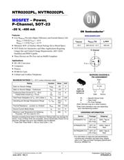
NTR0202PL, NVTR0202PL
MOSFET – Power,
P-Channel, SOT-23
-20 V, -400 mA
Features
• Low R
DS(on)
Provides Higher Efficiency and Extends Battery Life
R
DSon
= 0.80 W, V
GS
= −10 V
R
DSon
= 1.10 W, V
GS
= −4.5 V
• Miniature SOT−23 Surface Mount Package Saves Board Space
• NVT Prefix for Automotive and Other Applications Requiring
Unique Site and Control Change Requirements; AEC−Q101
Qualified and PPAP Capable
• These Devices are Pb−Free and are RoHS Compliant
Applications
• DC−DC Converters
• Computers
• Printers
• PCMCIA Cards
• Cellular and Cordless Telephones
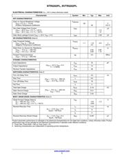
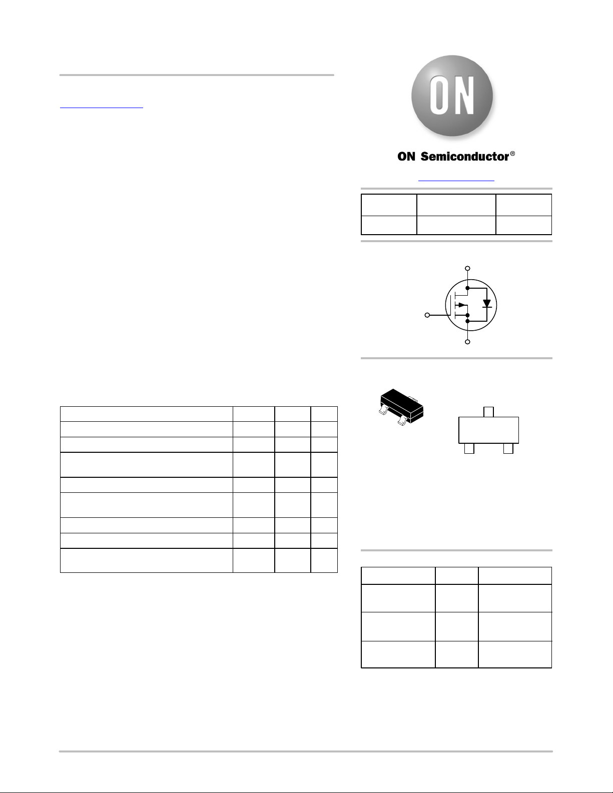
MAXIMUM RATINGS (T
J
= 25°C unless otherwise noted)
Rating
Symbol Value Unit
Drain−to−Source Voltage V
DSS
−20 V
Gate−to−Source Voltage − Continuous V
GS
$20 V
Continuous Drain Current @ T
A
= 25°C
Pulsed Drain Current (t
p
≤ 10 ms)
I
D
I
DM
−0.4
−1.0
A
Total Power Dissipation @ T
A
= 25°C (Note 1) P
D
225 mW
Operating and Storage Temperature Range T
J
, T
stg
− 55 to
150
°C
Thermal Resistance − Junction−to−Ambient
R
q
JA
556 °C/W
Source Current (Body Diode) I
S
0.4 A
Maximum Lead Temperature for Soldering
Purposes, 1/8″ from case for 10 s
T
L
260 °C
Stresses exceeding those listed in the Maximum Ratings table may damage the
device. If any of these limits are exceeded, device functionality should not be
assumed, damage may occur and reliability may be affected.
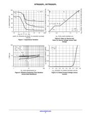
1. Pulse Test: Pulse Width v 300 ms, Duty Cycle v 2%.
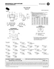
Device Package Shipping
†
ORDERING INFORMATION
−20 V
550 mW @ −10 V
R
DS(on)
Typ
−400 mA
I
D
MAXV
(BR)DSS
†For information on tape and reel specifications,
including part orientation and tape sizes, please
refer to our Tape and Reel Packaging Specification
Brochure, BRD8011/D.
NTR0202PLT3G SOT−23
(Pb−Free)
10000 / Tape &
Reel
NTR0202PLT1G SOT−23
(Pb−Free)
3000 / Tape &
Reel
D
G
S
P−Channel
SOT−23
CASE 318
STYLE 21
MARKING DIAGRAM &
PIN ASSIGNMENT
PL = Specific Device Code
M = Date Code*
G = Pb−Free Package
(Note: Microdot may be in either location)
*Date Code orientation may vary depending
upon manufacturing location.
PL M G
G
1
Gate
2
Source
Drain
3
NVTR0202PLT1G SOT−23
(Pb−Free)
3000 / Tape &
Reel
www.onsemi.com
器件 Datasheet 文档搜索
AiEMA 数据库涵盖高达 72,405,303 个元件的数据手册,每天更新 5,000 多个 PDF 文件
