Datasheet 搜索 > MOS管 > ON Semiconductor(安森美) > NTR4101PT1G 数据手册 > NTR4101PT1G 产品手册 1/5 页

¥ 0.327
NTR4101PT1G 产品手册 - ON Semiconductor(安森美)
制造商:
ON Semiconductor(安森美)
分类:
MOS管
封装:
SOT-23-3
描述:
ON SEMICONDUCTOR NTR4101PT1G 晶体管, MOSFET, P沟道, 3.2 A, -20 V, 0.07 ohm, -4.5 V, -720 mV
Pictures:
3D模型
符号图
焊盘图
引脚图
产品图
页面导航:
导航目录
NTR4101PT1G数据手册
Page:
of 5 Go
若手册格式错乱,请下载阅览PDF原文件
© Semiconductor Components Industries, LLC, 2010
June, 2010 − Rev. 5
1 Publication Order Number:
NTR4101P/D
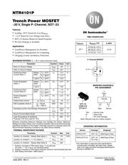
NTR4101P
Trench Power MOSFET
−20 V, Single P−Channel, SOT−23
Features
• Leading −20 V Trench for Low R
DS(on)
• −1.8 V Rated for Low Voltage Gate Drive
• SOT−23 Surface Mount for Small Footprint
• Pb−Free Package is Available
Applications
• Load/Power Management for Portables
• Load/Power Management for Computing
• Charging Circuits and Battery Protection
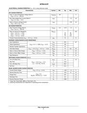
MAXIMUM RATINGS (T
J
= 25°C unless otherwise noted)
Parameter Symbol Value Unit
Drain−to−Source Voltage V
DSS
−20 V
Gate−to−Source Voltage V
GS
±8.0 V
Continuous Drain
Current (Note 1)
Steady
State
T
A
= 25°C
I
D
−2.4
A
T
A
= 85°C −1.7
t ≤10 s T
A
= 25°C −3.2
Power Dissipation
(Note 1)
Steady
State
T
A
= 25°C P
D
0.73
W
t ≤10 s 1.25
Continuous Drain
Current (Note 2)
Steady
State
T
A
= 25°C
I
D
−1.8
A
T
A
= 85°C −1.3
Power Dissipation
(Note 2)
T
A
= 25°C P
D
0.42 W
Pulsed Drain Current
tp =10 ms
I
DM
−18 A
ESD Capability (Note 3) C = 100 pF,
RS = 1500 W
ESD 225 V
Operating Junction and Storage Temperature T
J
,
T
STG
−55 to
150
°C
Source Current (Body Diode) I
S
−2.4 A
Lead Temperature for Soldering
Purposes (1/8” from case for 10 s)
T
L
260 °C
Stresses exceeding Maximum Ratings may damage the device. Maximum
Ratings are stress ratings only. Functional operation above the Recommended
Operating Conditions is not implied. Extended exposure to stresses above the
Recommended Operating Conditions may affect device reliability.
THERMAL RESISTANCE RATINGS
Parameter Symbol Max Unit
Junction−to−Ambient − Steady State (Note 1)
R
q
JA
170
°C/W
Junction−to−Ambient − t < 10 s (Note 1)
R
q
JA
100
Junction−to−Ambient − Steady State (Note 2)
R
q
JA
300
1. Surface−mounted on FR4 board using 1 in sq pad size
(Cu area = 1.127 in sq [1 oz] including traces)
2. Surface−mounted on FR4 board using the minimum recommended pad size.
3. ESD Rating Information: HBM Class 0
S
G
D
Device Package Shipping
†
ORDERING INFORMATION
NTR4101PT1 SOT−23 3000/Tape & Reel
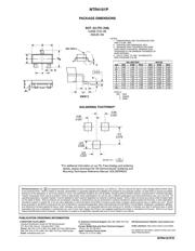
P−Channel MOSFET
SOT−23
CASE 318
STYLE 21
TR4 MG
G
TR4 = Device Code
M = Date Code
G = Pb−Free Package
MARKING DIAGRAM &
PIN ASSIGNMENT
3
Drain
1
Gate
2
1
3
2
Source
NTR4101PT1G
http://onsemi.com
SOT−23
Pb−Free
3000/Tape & Reel
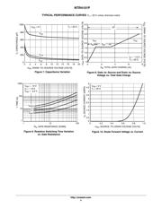
V
(BR)DSS
R
DS(ON)
TYP I
D
MAX
−20 V
70 mW @ −4.5 V
90 mW @ −2.5 V
112 mW @ −1.8 V
−3.2 A
†For information on tape and reel specifications,
including part orientation and tape sizes, please
refer to our Tape and Reel Packaging Specifications
Brochure, BRD8011/D.
http://onsemi.com
(Note: Microdot may be in either location)
器件 Datasheet 文档搜索
AiEMA 数据库涵盖高达 72,405,303 个元件的数据手册,每天更新 5,000 多个 PDF 文件
