Datasheet 搜索 > 运算放大器 > ADI(亚德诺) > OP495GP 数据手册 > OP495GP 其他数据使用手册 4/12 页

¥ 19.364
OP495GP 其他数据使用手册 - ADI(亚德诺)
制造商:
ADI(亚德诺)
分类:
运算放大器
封装:
PDIP
描述:
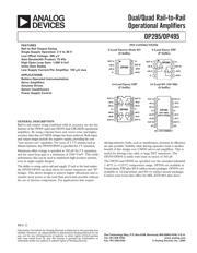
双/四路轨到轨运算放大器 DUAL/QUAD RAIL-TO-RAIL OPERATIONAL AMPLIFIERS
Pictures:
3D模型
符号图
焊盘图
引脚图
产品图
页面导航:
功能描述在P1
技术参数、封装参数在P2P3
应用领域在P1P7
电气规格在P2P3
导航目录
OP495GP数据手册
Page:
of 12 Go
若手册格式错乱,请下载阅览PDF原文件
REV. C
–4–
OP295/OP495
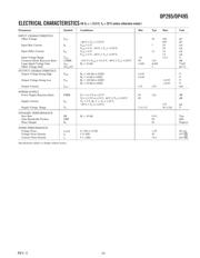
ABSOLUTE MAXIMUM RATINGS
1
Supply Voltage . . . . . . . . . . . . . . . . . . . . . . . . . . . . . . . . .±18 V
Input Voltage
2
. . . . . . . . . . . . . . . . . . . . . . . . . . . . . . . . . ±18 V
Differential Input Voltage
2
. . . . . . . . . . . . . . . . . . . . . . . . . 36 V
Output Short-Circuit Duration . . . . . . . . . . . . . . . . . Indefinite
Storage Temperature Range
P, S Package . . . . . . . . . . . . . . . . . . . . . . . . –65∞C to +150∞C
Operating Temperature Range
OP295G, OP495G . . . . . . . . . . . . . . . . . . . –40∞C to +125∞C
Junction Temperature Range
P, S Package . . . . . . . . . . . . . . . . . . . . . . . . –65∞C to +150∞C
Lead Temperature Range (Soldering, 60 Sec) . . . . . . . . 300∞C
NOTES
1
Absolute maximum ratings apply to packaged parts, unless otherwise noted.
2
For supply voltages less than ± 18 V, the absolute maximum input voltage is
equal to the supply voltage.
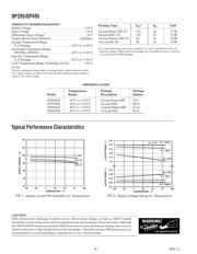
Typical Performance Characteristics
140
20
100
80
40
–25
60
–50
120
100
7550250
TEMPERATURE – ⴗC
SUPPLY CURRENT – A
V
S
= 5V
V
S
= 3V
V
S
= 36V
TPC 1. Supply Current Per Amplifier vs. Temperature
Package Type
JA
*
JC
Unit
8-Lead Plastic DIP (P) 103 43 ∞C/W
8-Lead SOIC (S) 158 43 ∞ C/W
14-Lead Plastic DIP (P) 83 39 ∞C/W
16-Lead SO (S) 98 30 ∞C/W
*q
JA
is specified for the worst case conditions, i.e., q
JA
is specified for device in
socket for cerdip, P-DIP, and LCC packages; q
JA
is specified for device soldered
in circuit board for SOIC package.
ORDERING GUIDE
Temperature Package Package
Model Range Description Option
OP295GP –40∞C to +125∞C 8-Lead Plastic DIP N-8
OP295GS –40∞C to +125∞C 8-Lead SOIC SO-8
OP495GP –40∞C to +125∞C 14-Lead Plastic DIP N-14
OP495GS –40∞C to +125∞C 16-Lead SOL R-16
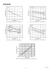
15.2
–15.2
100
–14.6
–15.0
–25
–14.8
–50
14.2
–14.4
14.4
14.6
14.8
15.0
7550250
TEMPERATURE –
C
– OUTPUT SWING – V + OUTPUT SWING – V
V
S
= 15V
R
L
= 100k⍀
R
L
= 2k⍀
R
L
= 10k⍀
R
L
= 2k⍀
R
L
= 10k⍀
R
L
= 100k⍀
TPC 2. Output Voltage Swing vs. Temperature
CAUTION
ESD (electrostatic discharge) sensitive device. Electrostatic charges as high as 4000 V readily
accumulate on the human body and test equipment and can discharge without detection. Although
the OP295/OP495 features proprietary ESD protection circuitry, permanent damage may occur on
devices subjected to high-energy electrostatic discharges. Therefore, proper ESD precautions are
recommended to avoid performance degradation or loss of functionality.
WARNING!
ESD SENSITIVE DEVICE
器件 Datasheet 文档搜索
AiEMA 数据库涵盖高达 72,405,303 个元件的数据手册,每天更新 5,000 多个 PDF 文件
