Datasheet 搜索 > 接口芯片 > NXP(恩智浦) > PCA9511D,112 数据手册 > PCA9511D,112 其他数据使用手册 5/18 页

 器件3D模型
¥ 0
PCA9511D,112 其他数据使用手册 - NXP(恩智浦)
制造商:
NXP(恩智浦)
分类:
接口芯片
封装:
SOIC-8
描述:
缓冲器和线路驱动器 HOT SWAP I2C/SMBUS BUS BUFFER
Pictures:
3D模型
符号图
焊盘图
引脚图
产品图
页面导航:

导航目录
PCA9511D,112数据手册
Page:
of 18 Go
若手册格式错乱,请下载阅览PDF原文件
NXP Semiconductors Product data sheet
PCA9511Hot swappable I
2
C-bus and SMBus bus buffer
2009 May 08
5
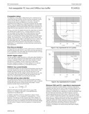
OPERATION
Start-up
An under voltage/initialization circuit holds the parts in a
disconnected state which presents high-impedance to all SDA and
SCL pins during power-up. A LOW on the ENABLE pin also forces
the parts into the low current disconnected state when the I
CC
is
essentially zero. As the power supply is brought up and the
ENABLE is HIGH or the part is powered and the ENABLE is taken
from LOW to HIGH, it enters an initialization state where the internal
references are stabilized and the precharge circuit for PCA9511 is
enabled. At the end of the initialization state the “Stop Bit And Bus
Idle” detect circuit is enabled. With the ENABLE pin HIGH long
enough to complete the initialization state and remaining HIGH
when all the SDA and SCl pins have been HIGH for the bus idle
time, or when all pins are HIGH and a STOP condition is seen on
the SDAIN and SCLIN pins, SDAIN is connected to SDAOUT and
SCLIN is connected to SCLOUT. The 1 V precharge circuitry is
activated during the initialization and is deactivated when the
connection is made. The precharge circuitry pulls up the SDA and
SCL pins to 1 V through individual 100 kΩ nominal resistors. This
precharges the pins to 1 V to minimize the worst-case disturbances
that result from inserting a card into the backplane where the
backplane and the card are at opposite logic levels.
Connect circuitry
Once the connection circuitry is activated, the behavior of SDAIN
and SDAOUT as well as SCLIN and SCLOUT become identical with
each acting as a bidirectional buffer that isolates the input
capacitance from the output bus capacitance while communicating
the logic levels. A LOW forced on either SDAIN or SDAOUT will
cause the other pin to be driven to a LOW by the part. The same is
also true for the SCL pins. Noise between 0.7V
CC
and V
CC
is
generally ignored because a falling edge is only recognized when it
falls below 0.7V
CC
with a slew rate of at least 1.25 V/µs. When a
falling edge is seen on one pin the other pin in the pair turns on a
pull-down driver that is referenced to a small voltage above the
falling pin. The driver will pull the pin down at a slew rate determined
by the driver and the load initially, because it does not start until the
first falling pin is below 0.7V
CC
. The first falling pin may have a fast
or slow slew rate, if it is faster than the pull down slew rate then the
initial pull down rate will continue. If the first falling pin has a slow
slew rate then the second pin will be pulled down at its initial slew
rate only until it is just above the first pin voltage the they will both
continue down at the slew rate of the first.
Once both sides are LOW they will remain LOW until all the external
drivers have stopped driving LOWs. If both sides are being driven
LOW to the same value for instance, 10 mV by external drivers,
which is the case for clock stretching and is typically the case for
acknowledge, and one side external driver stops driving that pin will
rise and rise above the nominal offset voltage until the internal driver
catches up and pulls it back down to the offset voltage. This bounce
is worst for low capacitances and low resistances, and may become
excessive. When the last external driver stops driving a LOW, that
pin will bounce up and settle out out just above the other pin as both
rise together with a slew rate determined by the internal slew rate
control and the RC time constant. As long as the slew rate is at least
1.25 V/µs, when the pin voltage exceeds 0.6 V, the rise time
accelerators circuits are turned on and the pull down driver is turned
off.
Maximum number of devices in series
Each buffer adds about 0.065 V dynamic level offset at 25 °C with
the offset larger at higher temperatures. Maximum offset (V
OS
) is
0.150 V. The LOW level at the signal origination end (master) is
dependent upon the load and the only specification point is the
I
2
C-bus specification of 3 mA will produce V
OL
< 0.4 V, although if
lightly loaded the V
OL
may be ∼0.1 V. Assuming V
OL
= 0.1 V and
V
OS
= 0.1 V, the level after four buffers would be 0.5 V, which is only
about 0.1 V below the threshold of the rising edge accelerator (about
0.6 V). With great care a system with four buffers may work, but as
the V
OL
moves up from 0.1 V, noise or bounces on the line will result
in firing the rising edge accelerator thus introducing false clock
edges. Generally it is recommended to limit the number of buffers in
series to two.
The PCA9510 (rise time accelerator is permanently disabled) and
the PCA9512 (rise time accelerator can be turned off) are a little
different with the rise time accelerator turned off because the rise
time accelerator will not pull the node up, but the same logic that
turns on the accelerator turns the pull-down off. If the V
IL
is above
∼0.6 V and a rising edge is detected, the pull-down will turn off and
will not turn back on until a falling edge is detected; so if the noise is
small enough it may be possible to use more than two PCA9510 or
PCA9512 parts in series, but is not recommended.
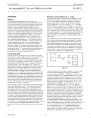
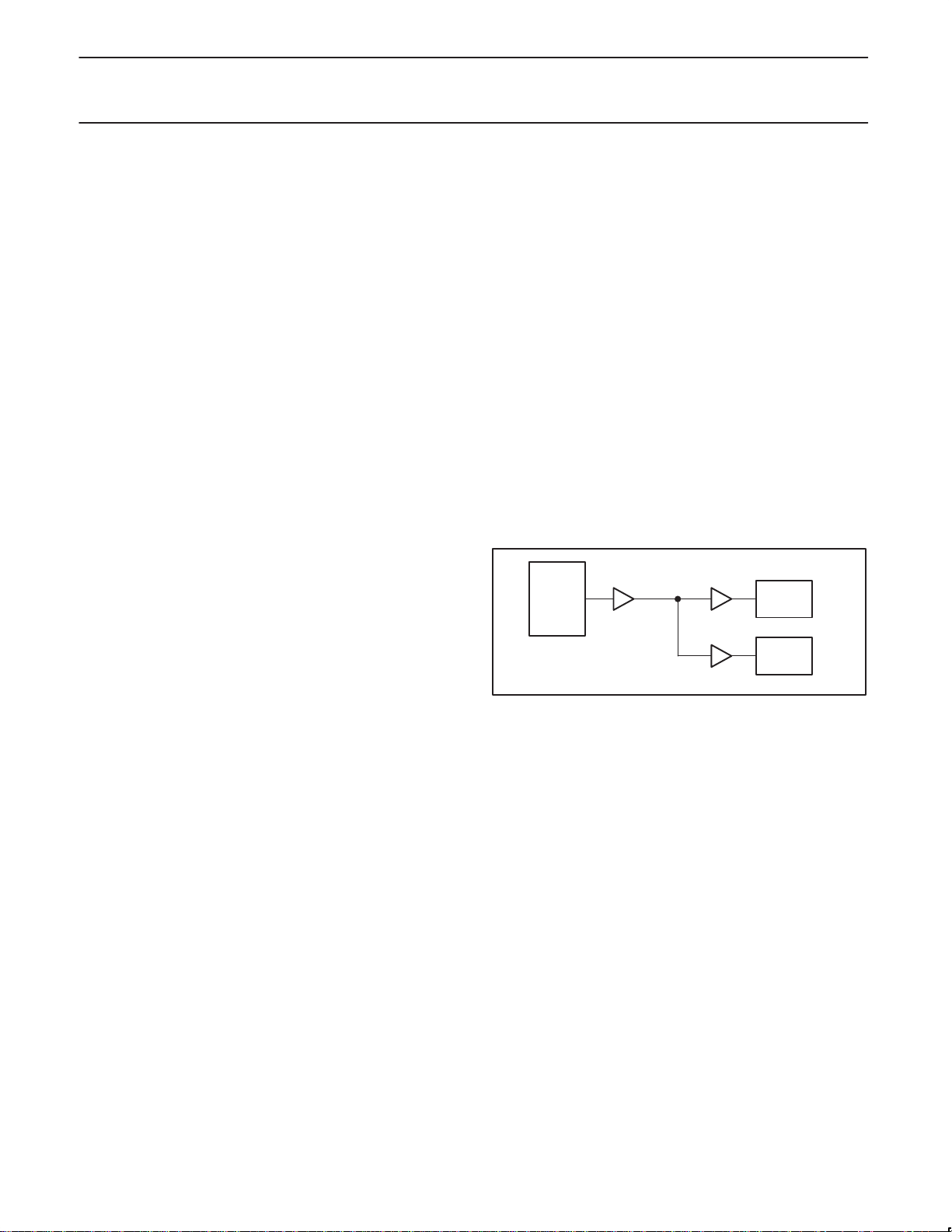
MASTER
buffer A
SLAVE B
buffer B
SLAVE C
buffer C
SW02353
common
node
Figure 4.
Consider a system with three buffers connected to a common node
and communication between the Master and Slave B that are
connected at either end of Buffer A and Buffer B in series as shown
in Figure 4. Consider if the V
OL
at the input of Buffer A is 0.3 V and
the V
OL
of Slave B (when acknowledging) is 0.4 V with the direction
changing from Master to Slave B and then from Slave B to Master.
Before the direction change you would observe V
IL
at the input of
Buffer A of 0.3 V and its output, the common node, is ∼0.4 V. The
output of Buffer B and Buffer C would be ∼0.5 V, but Slave B is
driving 0.4 V, so the voltage at Slave B is 0.4 V. The output of
Buffer C is ∼0.5 V. When the Master pull-down turns off, the input of
Buffer A rises and so does its output, the common node, because it
is the only part driving the node. The common node will rise to 0.5 V
before Buffer B’s output turns on, if the pull-up is strong the node will
bounce. If the bounce goes above the threshold for the rising edge
accelerator ∼0.6 V the accelerators on both Buffer A and Buffer C
will fire contending with the output of Buffer B. The node on the input
of Buffer A will go HIGH as will the input node of Buffer C. After the
common node voltage is stable for a while the rising edge
accelerators will turn off and the common node will return to ∼0.5 V
because the Buffer B is still on. The voltage at both the Master and
Slave C nodes would then fall to ∼0.6 V until Slave B turned off. This
would not cause a failure on the data line as long as the return to
0.5 V on the common node (∼0.6 V at the Master and Slave C)
occurred before the data setup time. If this were the SCL line, the
parts on Buffer A and Buffer C would see a false clock rather than a
stretched clock, which would cause a system error.
器件 Datasheet 文档搜索
AiEMA 数据库涵盖高达 72,405,303 个元件的数据手册,每天更新 5,000 多个 PDF 文件
