Datasheet 搜索 > 时钟缓冲器、驱动器、锁相环 > Pericom Semiconductor(百利通) > PI6C48545LEX 数据手册 > PI6C48545LEX 其他数据使用手册 1/5 页
 器件3D模型
¥ 10.535
PI6C48545LEX 其他数据使用手册 - Pericom Semiconductor(百利通)
制造商:
Pericom Semiconductor(百利通)
分类:
时钟缓冲器、驱动器、锁相环
封装:
TSSOP-20
Pictures:
3D模型
符号图
焊盘图
引脚图
产品图
页面导航:

导航目录
PI6C48545LEX数据手册
Page:
of 5 Go
若手册格式错乱,请下载阅览PDF原文件
1
PS8770 06/23/05
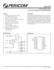
PI6C48545
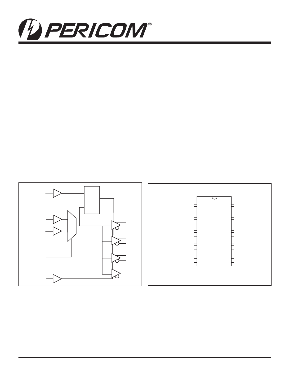
Block Diagram
Features
• Maximum operation frequency: 650 MHz
• 4 pair of differential LVDS outputs
• Selectable CLK
0
and CLK
1
inputs
• CLK
0
, CLK
1
accept LVCMOS, LVTTL input level
• Output Skew: 40ps (maximum)
• Part-to-part skew: 300ps (maximum)
• Propagation delay: 2.2ns (maximum)
• 3.3V power supply
• Pin-to-pin compatible to ICS8545
• Operating Temperature: -40
o
C to 85
o
C
• Packaging (Pb-free & Green):
- 20-pin TSSOP (L)
3.3V Low Skew 1-to-4
LVTTL/LVCMOS to LVDS Fanout Buffer
Description
The PI6C48545 is a high-performance low-skew LVDS fanout
buffer. PI6C48545 features two selectable single-ended clock in-
puts and translate to four LVDS outputs. The CLK
0
and CLK
1
inputs accept LVCMOS or LVTTL signals. The outputs are
synchronized with input clock during asynchronous assertion/
deassertion of CLK_EN pin. PI6C48545 is ideal for single-ended
LVTTL/LVCMOS to LVDS translations. Typical clock transla-
tion and distribution applications are data-communications and
telecommunications.
Pin Diagram
CLK_EN
CLK
0
CLK
1
CLK_SEL
OE
Q
3
n
Q
3
Q
1
n
Q
1
Q
2
n
Q
2
Q
0
n
Q
0
0
1
D
LE
Q
GND
CLK_EN
CLK_SEL
CLK
0
NC
CLK
1
NC
OE
GND
V
CC
Q
0
nQ
0
V
CC
Q
1
nQ
1
Q
2
nQ
2
GND
Q
3
nQ
3
1
2
3
4
5
6
7
8
9
10
20
19
18
17
16
15
14
13
12
11
器件 Datasheet 文档搜索
AiEMA 数据库涵盖高达 72,405,303 个元件的数据手册,每天更新 5,000 多个 PDF 文件
