Datasheet 搜索 > 实时时钟芯片 > Epson Electronics(爱普生) > RX8900SA:UC3 PURE SN 数据手册 > RX8900SA:UC3 PURE SN 其他数据使用手册 6/44 页
 器件3D模型
¥ 5.097
RX8900SA:UC3 PURE SN 其他数据使用手册 - Epson Electronics(爱普生)
制造商:
Epson Electronics(爱普生)
分类:
实时时钟芯片
封装:
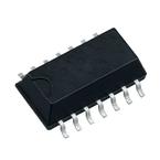
SOIC-14
Pictures:
3D模型
符号图
焊盘图
引脚图
产品图
页面导航:
引脚图在P6Hot
原理图在P5
技术参数、封装参数在P7
电气规格在P8
导航目录
RX8900SA:UC3 PURE SN数据手册
Page:
of 44 Go
若手册格式错乱,请下载阅览PDF原文件
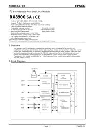
RX8900 SA / CE
Page - 3 ETM45E-03
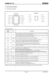
3. Terminal description
3.1. Terminal connections
RX8900SA
1. T1 (CE)
14.
N.C.
2. SCL
13.
SDA
3. FOUT
12.
T2 (VPP)
4. N.C. 11. GND
5. VBAT
10.
/ INT
6. VDD
9.
N.C.
7. FOE
8.
N.C.
SOP
−
14pin
RX8900CE
1. FOE
10.
/ INT
2. V
DD
9.
GND
3. V
BAT
8.
T2
(V
PP
)
4. FOUT
7
.
SDA
5. SCL 6
.
T1
(CE)
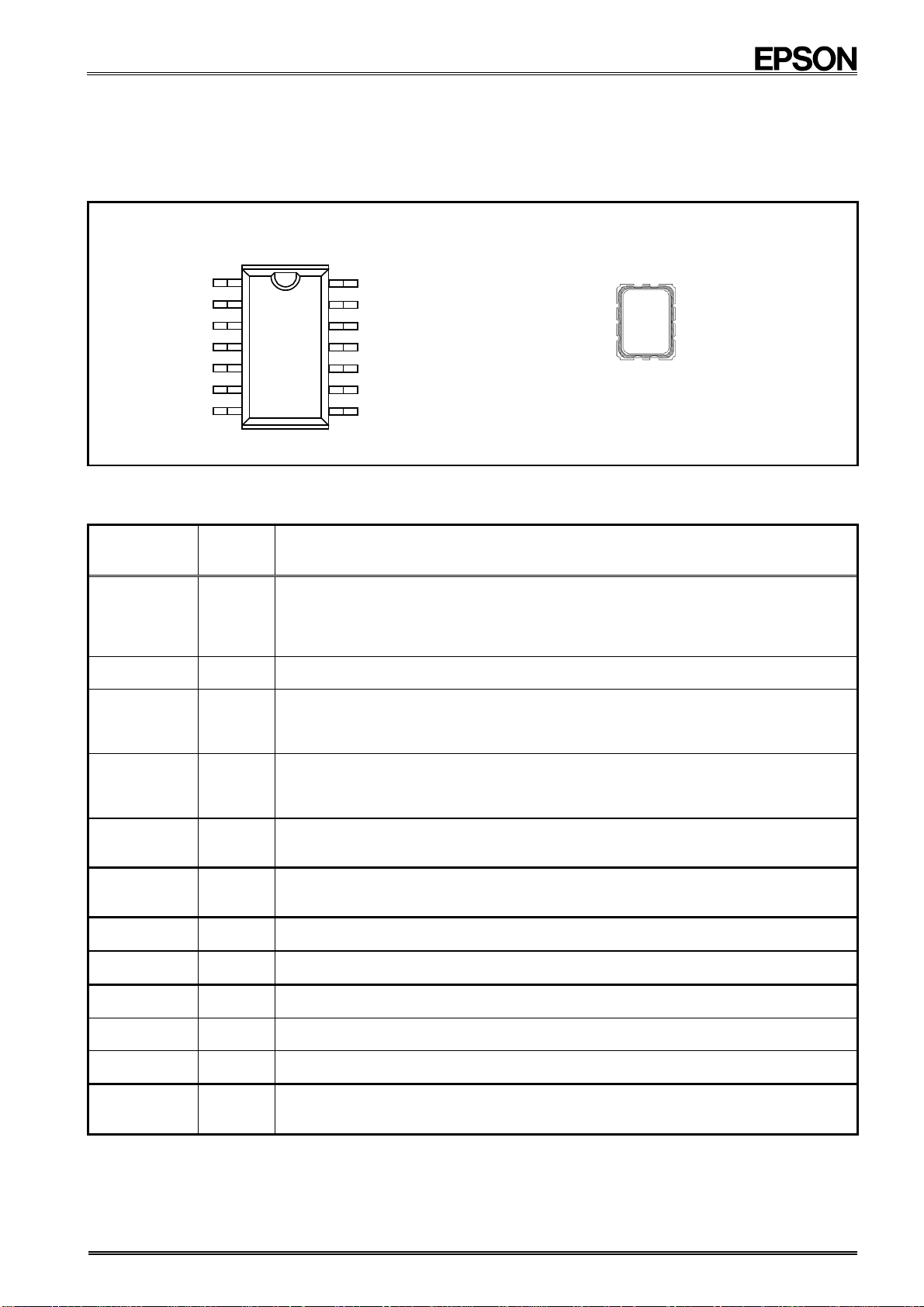
3.2. Pin Functions
Signal
name
I/O Function
SDA I/O
This pin's signal is used for input and output of address, data, and ACK bits, synchronized
with the serial clock used for I
2
C communications.
Since the SDA pin is an N-ch open drain pin during output, be sure to connect a suitable
pull-up resistance relative to the signal line capacity.
SCL Input This is the serial clock input pin for I
2
C Bus communications.
FOUT Output
This is the C-MOS output pin with output control provided via the FOE pin.
When FOE = "H" (high level), this pin outputs a 32.768 kHz signal.
When output is stopped, the FOUT pin = "Hi-Z"( high impedance ).
FOE Input
This is an input pin used to control the output mode of the FOUT pin.
When this pin's level is high, the FOUT pin is in output mode.
When it is low, output via the
FOUT pin is stopped.
/ INT Output
This pins is used to output alarm signals, timer signals, time update signals, and other
signals. This pin is an open drain pin.
V
BAT
−
This is a power supply pin for backup battery.
This is a pin to connect a large-capacity capacitor, a secondary battery.
When the battery switchover function does not need, VBAT must be connected to VDD.
V
DD
−
This pin is connected to a positive power supply.
GND
−
This pin is connected to a ground.
TEST Input Use by the manufacture for testing. ( Do not connect externally.)
T1 (CE) Input Use by the manufacture for testing. ( Do not connect externally.)
T2 (V
PP
)
−
Use by the manufacture for testing. ( Do not connect externally.)
N.C.
−
This pin is not connected to the internal IC.
Leave N.C. pins open or connect them to GND or V
DD
.
Note: Be sure to connect a bypass capacitor rated at least 0.1 µF between V
DD
and GND, V
BAT
and GND.
器件 Datasheet 文档搜索
AiEMA 数据库涵盖高达 72,405,303 个元件的数据手册,每天更新 5,000 多个 PDF 文件
