Datasheet 搜索 > 齐纳二极管 > ON Semiconductor(安森美) > SZMMSZ4705T1G 数据手册 > SZMMSZ4705T1G 产品封装文件 1/6 页
 器件3D模型
¥ 0.369
SZMMSZ4705T1G 产品封装文件 - ON Semiconductor(安森美)
制造商:
ON Semiconductor(安森美)
分类:
齐纳二极管
封装:
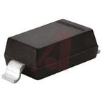
SOD-123-2
描述:
Zener Diodes, ON Semiconductor
Pictures:
3D模型
符号图
焊盘图
引脚图
产品图
页面导航:
导航目录
SZMMSZ4705T1G数据手册
Page:
of 6 Go
若手册格式错乱,请下载阅览PDF原文件
Semiconductor Components Industries, LLC, 2012
February, 2012 − Rev. 9
1 Publication Order Number:
MMSZ4678T1/D
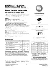
MMSZ4xxxT1G Series,
SZMMSZ4xxxT1G Series
Zener Voltage Regulators
500 mW SOD−123 Surface Mount
Three complete series of Zener diodes are offered in the convenient,
surface mount plastic SOD−123 package. These devices provide a
convenient alternative to the leadless 34−package style.
Features
500 mW Rating on FR−4 or FR−5 Board
Wide Zener Reverse Voltage Range − 1.8 V to 43 V
Package Designed for Optimal Automated Board Assembly
Small Package Size for High Density Applications
ESD Rating of Class 3 (> 16 kV) per Human Body Model
SZ Prefix for Automotive and Other Applications Requiring Unique
Site and Control Change Requirements; AEC−Q101 Qualified and
PPAP Capable
Pb−Free Packages are Available*
Mechanical Characteristics:
CASE:
Void-free, transfer-molded, thermosetting plastic case
FINISH: Corrosion resistant finish, easily solderable
MAXIMUM CASE TEMPERATURE FOR SOLDERING PURPOSES:
260C for 10 Seconds
POLARITY: Cathode indicated by polarity band
FLAMMABILITY RATING: UL 94 V−0
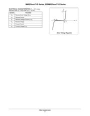
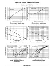
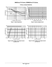
MAXIMUM RATINGS
Rating Symbol Max Units
Total Power Dissipation on FR−5 Board,
(Note 1) @ T
L
= 75C
Derated above 75C
P
D
500
6.7
mW
mW/C
Thermal Resistance, (Note 2)
Junction−to−Ambient
R
q
JA
340
C/W
Thermal Resistance, (Note 2)
Junction−to−Lead
R
q
JL
150
C/W
Junction and Storage Temperature Range T
J
, T
stg
−55 to
+150
C
Stresses exceeding Maximum Ratings may damage the device. Maximum
Ratings are stress ratings only. Functional operation above the Recommended
Operating Conditions is not implied. Extended exposure to stresses above the
Recommended Operating Conditions may affect device reliability.
1. FR−5 = 3.5 X 1.5 inches, using the minimum recommended footprint.
2. Thermal Resistance measurement obtained via infrared Scan Method.
*For additional information on our Pb−Free strategy and soldering details, please
download the ON Semiconductor Soldering and Mounting Techniques
Reference Manual, SOLDERRM/D.
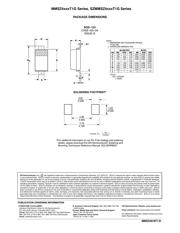
1
Cathode
2
Anode
See specific marking information in the device marking
column of the Electrical Characteristics table on page 3 of
this data sheet.
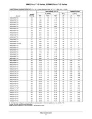
DEVICE MARKING INFORMATION
http://onsemi.com
SOD−123
CASE 425
STYLE 1
Device Package Shipping
†
ORDERING INFORMATION
MARKING DIAGRAM
†For information on tape and reel specifications,
including part orientation and tape sizes, please
refer to our Tape and Reel Packaging Specifications
Brochure, BRD8011/D.
MMSZ4xxxT1G SOD−123
(Pb−Free)
3,000 /
Tape & Reel
MMSZ4xxxT3G SOD−123
(Pb−Free)
10,000 /
Tape & Reel
xx = Device Code (Refer to page 3)
M = Date Code
G = Pb−Free Package
(Note: Microdot may be in either location)
xx M G
G
1
SZMMSZ4xxxT1G SOD−123
(Pb−Free)
3,000 /
Tape & Reel
SZMMSZ4xxxT3G SOD−123
(Pb−Free)
10,000 /
Tape & Reel
器件 Datasheet 文档搜索
AiEMA 数据库涵盖高达 72,405,303 个元件的数据手册,每天更新 5,000 多个 PDF 文件
