Datasheet 搜索 > 微处理器 > Microchip(微芯) > TS68040VF25A 数据手册 > TS68040VF25A 其他数据使用手册 1/49 页


¥ 0
TS68040VF25A 其他数据使用手册 - Microchip(微芯)
制造商:
Microchip(微芯)
分类:
微处理器
封装:
BCQFP-196
Pictures:
3D模型
符号图
焊盘图
引脚图
产品图
页面导航:
引脚图在P4P5Hot
原理图在P2
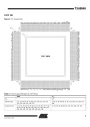
封装尺寸在P9P43
型号编码规则在P46
标记信息在P17
封装信息在P42
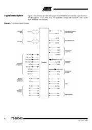
功能描述在P29
技术参数、封装参数在P9P19P20P21P22
电气规格在P9P11P18P19
导航目录
TS68040VF25A数据手册
Page:
of 49 Go
若手册格式错乱,请下载阅览PDF原文件
1
Features
• 26-42 MIPS Integer Performance
• 3.5-5.6 MFLOPS Floating-Point-Performance
• IEEE 754-Compatible FPU
• Independent Instruction and Data MMUs
• 4K bytes Physical Instruction Cache and 4K bytes Physical Data Cache Accessed
Simultaneously
• 32-bit, Nonmultiplexed External Address and Data Buses with Synchronous Interface
• User-Object-Code Compatibility with All Earlier TS68000 Microprocessors
• Multimaster/Multiprocessor Support via Bus Snooping
• Concurrent Integer Unit, FPU, MMU, Bus Controller, and Bus Snooper Maximize
Throughput
• 4G bytes Direct Addressing Range
• Software Support Including Optimizing C Compiler and UNIX
®
System V Port
• IEEE P 1149-1 Test Mode (JTAG)
• f = 25 MHz, 33 MHz; V
CC
= 5V ± 5%; P
D
= 7W
• The Use of the TS88915T Clock Driver is Suggested
Description
The TS68040 is Atmel’s third generation of 68000-compatible, high-performance, 32-
bit microprocessors. The TS68040 is a virtual memory microprocessor employing
multiple, concurrent execution units and a highly integrated architecture to provide
very high performance in a monolithic HCMOS device. On a single chip, the TS68040
integrates a 68030-compatible integer unit, an IEEE 754-compatible floating-point unit
(FPU), and fully independent instruction and data demand-paged memory manage-
ment units (MMUs), including 4K bytes independent instruction and data caches. A
high degree of instruction execution parallelism is achieved through the use of multi-
ple independent execution pipelines, multiple internal buses, and a full internal
Harvard architecture, including separate physical caches for both instruction and data
accesses. The TS68040 also directly supports cache coherency in multimaster appli-
cations with dedicated on-chip bus snooping logic.
The TS68040 is user-object-code compatible with previous members of the TS68000
Family and is specifically optimized to reduce the execution time of compiler-gener-
ated code. The 68040 HCMOS technology, provides an ideal balance between speed,
power, and physical device size.
Figure 1 is a simplified block diagram of the TS68040. Instruction execution is pipe-
lined in both the integer unit and FPU. Independent data and instruction MMUs control
the main caches and the address translation caches (ATCs). The ATCs speed up log-
ical-to-physical address translations by storing recently used translations. The bus
snooper circuit ensures cache coherency in multimaster and multiprocessing
applications.
Screening
•MIL-STD-883
• DESC. Drawing 5962-93143
• Atmel Standards
Third-
Generation
32-bit
Microprocessor
TS68040
Rev. 2116A–HIREL–09/02
器件 Datasheet 文档搜索
AiEMA 数据库涵盖高达 72,405,303 个元件的数据手册,每天更新 5,000 多个 PDF 文件
