Datasheet 搜索 > DA转换器 > ADI(亚德诺) > AD5624RBCPZ-5REEL7 数据手册 > AD5624RBCPZ-5REEL7 产品设计参考手册 1/28 页
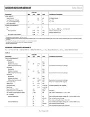
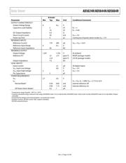
 器件3D模型
¥ 29.269
AD5624RBCPZ-5REEL7 产品设计参考手册 - ADI(亚德诺)
制造商:
ADI(亚德诺)
分类:
DA转换器
封装:
LFCSP-10
Pictures:
3D模型
符号图
焊盘图
引脚图
产品图
页面导航:

导航目录
AD5624RBCPZ-5REEL7数据手册
Page:
of 28 Go
若手册格式错乱,请下载阅览PDF原文件
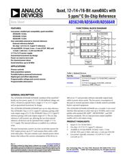
Quad, 12-/14-/16-Bit nanoDACs with
5 ppm/°C On-Chip Reference
Data Sheet
AD5624R/AD5644R/AD5664R
Rev. C Document Feedback
Information furnished by Analog Devices is believed to be accurate and reliable. However, no
responsibility is assumed by Analog Devices for its use, nor for any infringements of patents or other
rights of third parties that may result from its use. Specifications subject to change without notice. No
license is granted by implication or otherwise under any patent or patent rights of Analog Devices.
Trademarks and registered trademarks are the property of their respective owners.
One Technology Way, P.O. Box 9106, Norwood, MA 02062-9106, U.S.A.
Tel: 781.329.4700 ©2006–2013 Analog Devices, Inc. All rights reserved.
Technical Support www.analog.com
FEATURES
Low power, smallest pin-compatible, quad nanoDACs
AD5664R: 16 bits
AD5644R: 14 bits
AD5624R: 12 bits
User-selectable external or internal reference
External reference default
On-chip 1.25 V/2.5 V, 5 ppm/°C reference
10-lead MSOP; 10-lead, 3 mm × 3 mm LFCSP_WD; and
12-ball, 1.665 mm × 2.245 mm WLCSP
2.7 V to 5.5 V power supply
Guaranteed monotonic by design
Power-on reset to zero scale
Per channel power-down
Serial interface, up to 50 MHz
APPLICATIONS
Process controls
Data acquisition systems
Portable battery-powered instruments
Digital gain and offset adjustment
Programmable voltage and current sources
Programmable attenuators
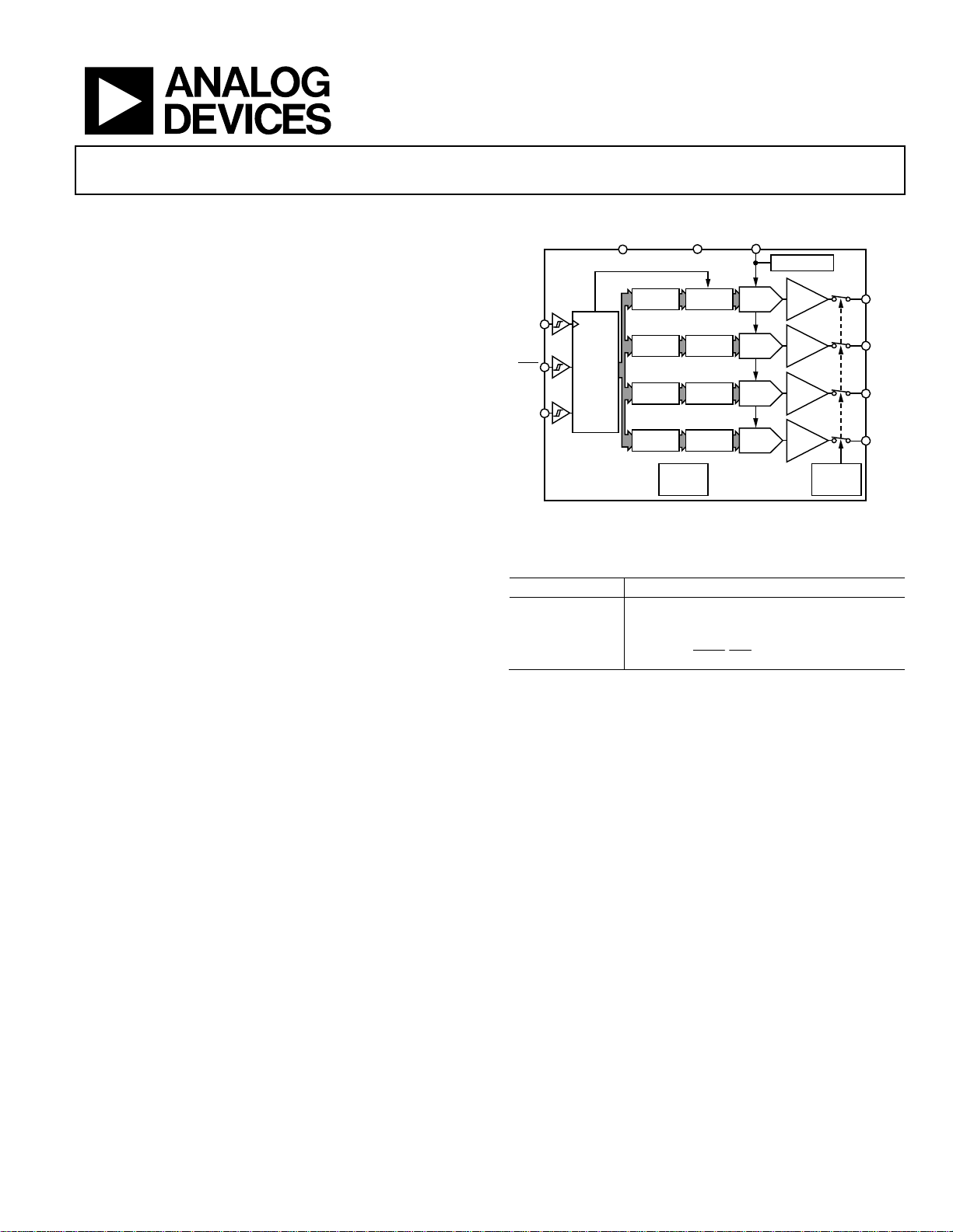
FUNCTIONAL BLOCK DIAGRAM
Figure 1.
Table 1. Related Devices
Part No. Description
AD5624/AD5664
2.7 V to 5.5 V quad, 12-/16-bit DACs, external
reference
AD5666
2.7 V to 5.5 V quad, 16-bit DAC, internal
reference, LDAC
, CLR pins
GENERAL DESCRIPTION
The AD5624R/AD5644R/AD5664R, members of the nanoDAC®
family, are low power, quad, 12-/14-/16-bit buffered voltage-out
DACs. All devices operate from a single 2.7 V to 5.5 V supply
and are guaranteed monotonic by design.
The AD5624R/AD5644R/AD5664R have an on-chip reference.
The AD56x4R-3 has a 1.25 V, 5 ppm/°C reference, giving a full-
scale output range of 2.5 V; the AD56x4R-5 has a 2.5 V, 5 ppm/°C
reference giving a full-scale output range of 5 V. The on-chip
reference is off at power-up, allowing the use of an external
reference; all devices can be operated from a single 2.7 V to
5.5 V supply. The internal reference is enabled via a software
write.
The part incorporates a power-on reset circuit that ensures the
DAC output powers up to 0 V and remains there until a valid
write takes place. The part contains a per-channel power-down
feature that reduces the current consumption of the device to
480 nA at 5 V and provides software-selectable output loads
while in power-down mode. The low power consumption of
this part in normal operation makes it ideally suited to portable
battery-operated equipment.
The AD5624R/AD5644R/AD5664R use a versatile 3-wire serial
interface that operates at clock rates up to 50 MHz, and is com-
patible with standard SPI, QSPI™, MICROWIRE™, and DSP
interface standards. The on-chip precision output amplifier
enables rail-to-rail output swing.
PRODUCT HIGHLIGHTS
1. Quad 12-/14-/16-bit DACs.
2. On-chip 1.25 V/2.5 V, 5 ppm/°C reference.
3. Available in 10-lead MSOP; 10-lead, 3 mm × 3 mm
LFCSP_WD; and 12-ball, 1.665 mm × 2.245 mm WLCSP.
4. Low power, typically consumes 1.32 mW at 3 V and
2.25 mW at 5 V.
0
5856-001
BUFFER
BUFFER
AD5624R/AD5644R/AD5664R
1.25V/2.5V REF
V
DD
V
REFIN
/
V
REFOUT
GND
POWER-
DOWN
LOGIC
POWER-ON
LOGIC
SCLK
S
YNC
DIN
STRING
DAC A
STRING
DAC B
STRING
DAC C
STRING
DAC D
DAC
REGISTER
DAC
REGISTER
DAC
REGISTER
DAC
REGISTER
INPUT
REGISTER
INPUT
REGISTER
INPUT
REGISTER
INPUT
REGISTER
INTERFACE
LOGIC
BUFFER
BUFFER
V
OUT
A
V
OUT
B
V
OUT
C
V
OUT
D
器件 Datasheet 文档搜索
AiEMA 数据库涵盖高达 72,405,303 个元件的数据手册,每天更新 5,000 多个 PDF 文件
