Datasheet 搜索 > DA转换器 > ADI(亚德诺) > AD5693RACPZ-RL7 数据手册 > AD5693RACPZ-RL7 产品设计参考手册 4/24 页
¥ 66.986
AD5693RACPZ-RL7 产品设计参考手册 - ADI(亚德诺)
制造商:
ADI(亚德诺)
分类:
DA转换器
封装:
LFCSP EP-8
描述:
16-位数模转换器-1-8-LFCSP-UD(2x2)
Pictures:
3D模型
符号图
焊盘图
引脚图
产品图
页面导航:
导航目录
AD5693RACPZ-RL7数据手册
Page:
of 24 Go
若手册格式错乱,请下载阅览PDF原文件

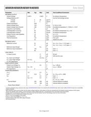
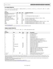
AD5693R/AD5692R/AD5691R/AD5693 Data Sheet
Parameter Min Typ Max Unit Test Conditions/Comments
REFERENCE OUTPUT
Output Voltage 2.4975 2.5025 V
At ambient temperature
Voltage Reference TC
3
See the Terminology section
A Grade 5 20 ppm/°C
B Grade
2
5
ppm/°C
Output Impedance 0.05 Ω
Output Voltage Noise 16.5 µV p-p
0.1 Hz to 10 Hz
Output Voltage Noise Density 240 nV/√Hz At ambient temperature, f = 10 kHz, C
L
= 10 nF
Capacitive Load Stability 5 µF R
L
= 2 kΩ
Load Regulation Sourcing 50 µV/mA At ambient temperature, V
DD
≥ 3 V
Load Regulation Sinking 30 µV/mA At ambient temperature
Output Current Load Capability
±5 mA V
DD
≥ 3 V
Line Regulation 80 µV/V At ambient temperature
Thermal Hysteresis 125 ppm First cycle
25 ppm Additional cycles
REFERENCE INPUT
Reference Current 35 µA V
REF
= V
DD
= V
LOGIC
= 5.5 V, gain = 1
57 µA V
REF
= V
DD
= V
LOGIC
= 5.5 V, gain = 2
Reference Input Range
4
V
DD
V
Reference Input Impedance 120 kΩ Gain = 1
60 kΩ Gain = 2
LOGIC INPUTS
I
IN
, Input Current
±1
µA Per pin
±3 µA SDA and SCL pins
V
INL
, Input Low Voltage
4
0.3 × V
DD
V
V
INH
, Input High Voltage
4
0.7 × V
DD
V
C
IN
, Pin Capacitance 2 pF
LOGIC OUTPUTS (SDA)
4
Output Low Voltage, V
OL
0.4 V I
SINK
= 200 μA
Output High Voltage, V
OH
V
DD
− 0.4 V I
SOURCE
= 200 μA
Pin Capacitance 4 pF
POWER REQUIREMENTS
V
LOGIC
5
1.8 5.5 V
I
LOGIC
5
0.25 3 µA V
IH
= V
LOGIC
or V
IL
= GND
V
DD
2.7 5.5 V Gain = 1
V
REF
+ 1.5 5.5 V Gain = 2
I
DD
6
V
IH
= V
DD
, V
IL
= GND
Normal Mode
7
350 500 µA Internal reference enabled
110 180 µA Internal reference disabled
Power-Down Modes
8
2 µA
1
Linearity calculated using a reduced code range: AD5693R/AD5693 (Code 512 to Code 65,535); AD5692R (Code 128 to Code 16,384); AD5691R (Code 32 to Code 4096).
Output unloaded.
2
When drawing a load current at either rail, the output voltage headroom, with respect to that rail, is limited by the 20 Ω typical channel resistance of the output
devices; for example, when sinking 1 mA, the minimum output voltage with 20 Ω, 1 mA generates 20 mV. See Figure 35 for more details.
3
Voltage reference temperature coefficient is calculated as per the box method. See the Terminology section for more information.
4
Substitute V
LOGIC
for V
DD
if the device includes a V
LOGIC
pin.
5
The V
LOGIC
pin is not available on all models.
6
If the V
LOGIC
pin is not available, I
DD
= I
DD
+ I
LOGIC
.
7
Interface inactive. DAC active. DAC output unloaded.
8
DAC powered down.
Rev. A | Page 4 of 24
器件 Datasheet 文档搜索
AiEMA 数据库涵盖高达 72,405,303 个元件的数据手册,每天更新 5,000 多个 PDF 文件

