Datasheet 搜索 > AD转换器 > ADI(亚德诺) > AD7785BRUZ-REEL 数据手册 > AD7785BRUZ-REEL 产品设计参考手册 6/32 页

 器件3D模型
¥ 54.957
AD7785BRUZ-REEL 产品设计参考手册 - ADI(亚德诺)
制造商:
ADI(亚德诺)
分类:
AD转换器
封装:
TSSOP-16
描述:
3通道,低噪声,低功耗, 20位⒉-ツADC,具有片内仪表放大器和基准 3-Channel, Low Noise, Low Power, 20-Bit ⒉-ツ ADC with On-Chip In-Amp and Reference
Pictures:
3D模型
符号图
焊盘图
引脚图
产品图
页面导航:
导航目录
AD7785BRUZ-REEL数据手册
Page:
of 32 Go
若手册格式错乱,请下载阅览PDF原文件
AD7785
Rev. 0 | Page 6 of 32
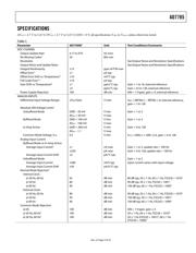
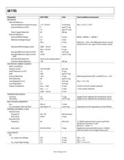
TIMING CHARACTERISTICS
AV
DD
= 2.7 V to 5.25 V, DV
DD
= 2.7 V to 5.25 V, GND = 0 V, Input Logic 0 = 0 V, Input Logic 1 = DV
DD
, unless otherwise noted.
Table 2.
Parameter
1, 2
Limit at T
MIN
, T
MAX
(B Version) Unit Conditions/Comments
t
3
100 ns min SCLK high pulse width
t
4
100 ns min SCLK low pulse width
Read Operation
t
1
0 ns min
CS falling edge to DOUT/RDY active time
60 ns max DV
DD
= 4.75 V to 5.25 V
80 ns max DV
DD
= 2.7 V to 3.6 V
t
2
3
0 ns min SCLK active edge to data valid delay
4
60 ns max DV
DD
= 4.75 V to 5.25 V
80 ns max DV
DD
= 2.7 V to 3.6 V
t
5
5, 6
10 ns min
Bus relinquish time after
CS inactive edge
80 ns max
t
6
0 ns min
SCLK inactive edge to
CS inactive edge
t
7
10 ns min
SCLK inactive edge to DOUT/
RDY high
Write Operation
t
8
0 ns min
CS falling edge to SCLK active edge setup time
4
t
9
30 ns min Data valid to SCLK edge setup time
t
10
25 ns min Data valid to SCLK edge hold time
t
11
0 ns min
CS rising edge to SCLK edge hold time
1
Sample tested during initial release to ensure compliance. All input signals are specified with t
R
= t
F
= 5 ns (10% to 90% of DV
DD
) and timed from a voltage level of 1.6 V.
2
See Figure 3 and Figure 4.
3
These numbers are measured with the load circuit shown in Figure 2 and defined as the time required for the output to cross the V
OL
or V
OH
limits.
4
SCLK active edge is the falling edge of SCLK.
5
These numbers are derived from the measured time taken by the data output to change 0.5 V when loaded with the circuit shown in Figure 2. The measured number
is then extrapolated back to remove the effects of charging or discharging the 50 pF capacitor. This means that the times quoted in the timing characteristics are the
true bus relinquish times of the part and, as such, are independent of external bus loading capacitances.
6
RDY
returns high after a read of the ADC. In single conversion mode and continuous conversion mode, the same data can be read again, if required, while
RDY
is high,
although care should be taken to ensure that subsequent reads do not occur close to the next output update. In continuous read mode, the digital word can be read
only once.
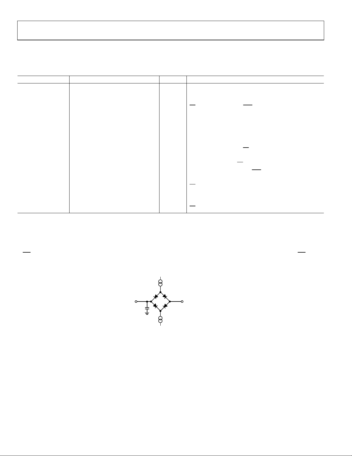
0
6721-002
I
SINK
(1.6mA WITH DV
DD
= 5V,
100µA WITH DV
DD
= 3V)
I
SOURCE
(200µA WITH DV
DD
= 5V,
100µA WITH DV
DD
= 3V)
1.6V
TO
OUTPUT
PIN
50pF
Figure 2. Load Circuit for Timing Characterization
器件 Datasheet 文档搜索
AiEMA 数据库涵盖高达 72,405,303 个元件的数据手册,每天更新 5,000 多个 PDF 文件
