Datasheet 搜索 > ADI(亚德诺) > AD9552 数据手册 > AD9552 产品设计参考手册 1/4 页


¥ 0
AD9552 产品设计参考手册 - ADI(亚德诺)
制造商:
ADI(亚德诺)
描述:
振荡器上变频器 Oscillator Frequency Upconverter
Pictures:
3D模型
符号图
焊盘图
引脚图
产品图
页面导航:
原理图在P3
导航目录
AD9552数据手册
Page:
of 4 Go
若手册格式错乱,请下载阅览PDF原文件
AN-1051
APPLICATION NOTE
One Technology Way • P. O. Box 9106 • Norwood, MA 02062-9106, U.S.A. • Te l: 781.329.4700 • Fax: 781.461.3113 • www.analog.com
Reference Design for the AD9552 Oscillator Frequency Upconverter
by Ken Gentile
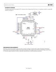
INTRODUCTION
The AD9552 is a low cost, programmable device that accepts
a low frequency input signal (between approximately 10 MHz
and 70 MHz) and upconverts it to a high frequency output
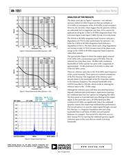
signal (up to 900 MHz). This application note provides a
reference design for the AD9552 and includes the performance
measurements of the output signal. It demonstrates that the
AD9552 (and all necessary supporting components) fits within
a 9 mm × 14 mm footprint—the same size as some currently
available oscillator packages. Refer to AN-0988 for additional
information on the features and function of the AD9552.
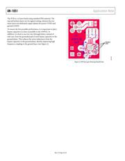
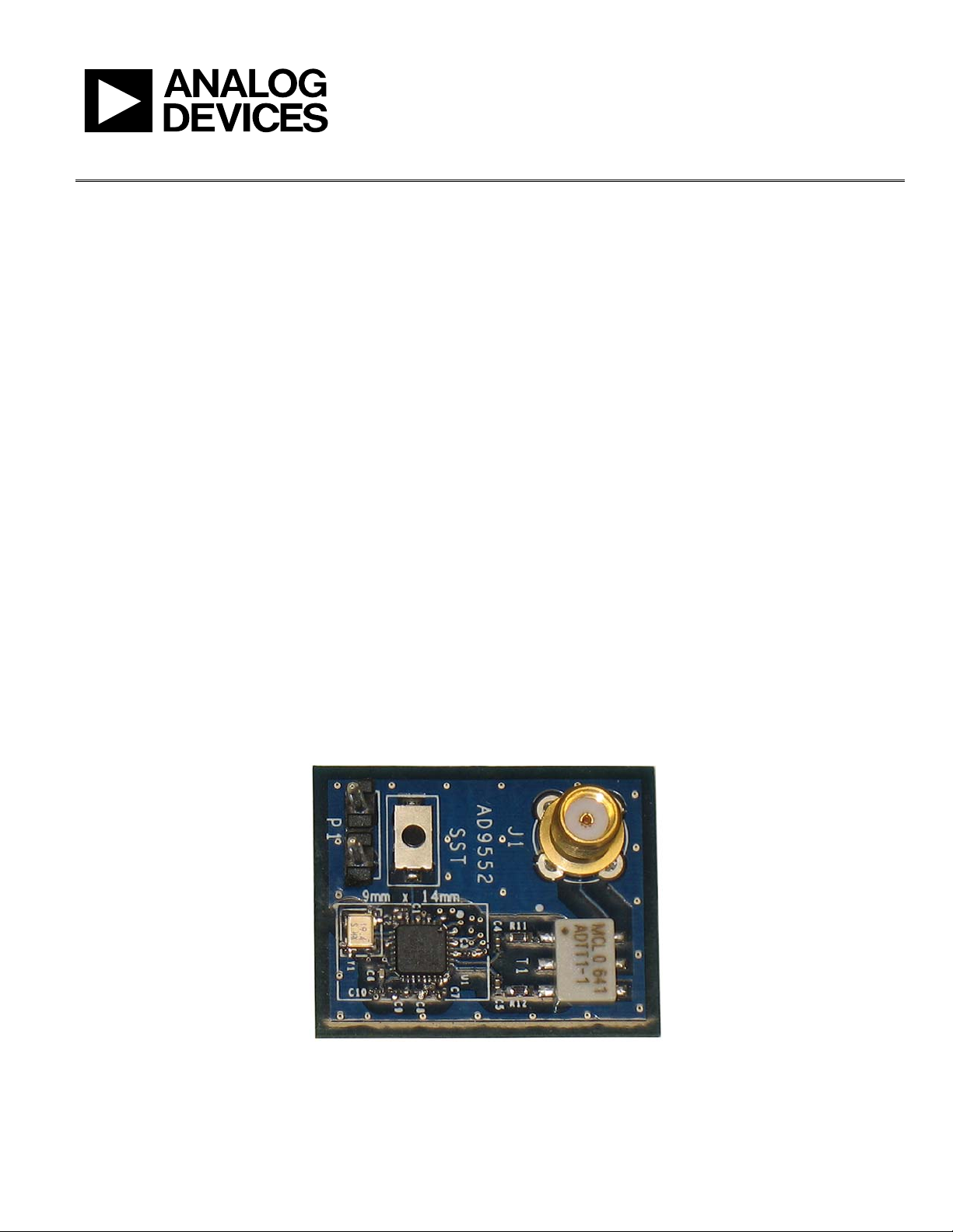
PRINTED CIRCUIT BOARD
A photograph of the 1” × 1.25” reference design circuit board
appears in Figure 1. Note the silkscreened 9 mm × 14 mm
rectangle, which contains the following:
• the AD9552
• a crystal resonator
• power supply bypass capacitors
• PLL loop filter components
These constitute all the necessary components to create an
oscillator frequency upconverter. The other components on the
PCB are strictly auxiliary. For instance, P1 in the upper left
corner serves only to bring power (3.3 V) to the board. Like-
wise, components J1, T1, C4, C5, R11, and R12 in the lower
right corner serve only as a convenient means of measuring the
AD9552 output signal. The switch (SST) to the right of P1 is
an auxiliary method for resetting the AD9952 (in lieu of cycling
the power). The bottom side of the PCB contains no compo-
nents other than pads for several grounding jumpers (0 Ω
resistors) to facilitate pin programming of the AD9552. The
reference design includes jumpers only to allow for different
crystal types or output frequencies. An end user application
typically consists of one crystal type and a fixed output
frequency. Thus, jumpers are not required on an end user
circuit board. Instead, one would route copper traces directly
from the appropriate programming pins to ground to select the
desired crystal frequency and output frequency for the specific
application.
This particular reference design uses a 19.44 MHz crystal
resonator with the AD9552 pin programmed for 625 MHz at
OUT1. Note that this demonstrates the ability of the AD9552
to perform noninteger frequency translation (19.44 MHz in,
625 MHz out). Furthermore, the design makes use of the
AD9552’s default output driver operating mode (LVPECL).
08639-001
Figure 1. AD9552 Reference Design PCB
Rev. 0 | Page 1 of 4
器件 Datasheet 文档搜索
AiEMA 数据库涵盖高达 72,405,303 个元件的数据手册,每天更新 5,000 多个 PDF 文件
