Datasheet 搜索 > 放大器、缓冲器 > ADI(亚德诺) > ADA4830-1BCPZ-R2 数据手册 > ADA4830-1BCPZ-R2 产品设计参考手册 1/8 页
 器件3D模型
¥ 5.601
ADA4830-1BCPZ-R2 产品设计参考手册 - ADI(亚德诺)
制造商:
ADI(亚德诺)
分类:
放大器、缓冲器
封装:
LFCSP-8
描述:
Analog DevicesAnalog Devices 的差分放大器经过集成和优化,适用于差分信号应用。 这些专业放大器具有固有的共模抑制特性,通过输出增益和相位匹配实现低谐波失真。 应用包括驱动或接收长电缆上的信号、驱动平衡 ADC 输入和查找互补输出。### 差动放大器### 差分放大器,Analog Devices
Pictures:
3D模型
符号图
焊盘图
引脚图
产品图
页面导航:
原理图在P3
型号编码规则在P5
功能描述在P1


导航目录
ADA4830-1BCPZ-R2数据手册
Page:
of 8 Go
若手册格式错乱,请下载阅览PDF原文件
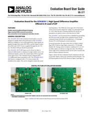
Evaluation Board User Guide
UG-377
One Technology Way • P. O. Box 9106 • Norwood, MA 02062-9106, U.S.A. • Te l: 781.329.4700 • Fax: 781.461.3113 • www.analog.com
Evaluation Board for the ADA4830-1, High Speed Difference Amplifier
Offered in 8-Lead LFCSP
PLEASE SEE THE LAST PAGE FOR AN IMPORTANT
WARNING AND LEGAL TERMS AND CONDITIONS.
Rev. 0 | Page 1 of 8
FEATURES
Enables quick breadboarding/prototyping
Edge-mounted SMA connector provisions
Easy connection to test equipment and other circuits
GENERAL DESCRIPTION
The ADA4830-1BCP-EBZ evaluation board makes it easy for
designers to quickly observe the performance of the ADA4830-1
difference amplifier in real-world applications. Input signals are
applied through SMA jacks (INP, INN), and the output is taken
from SMA Jack VOUT. Power is applied through the red +VS
pin. The black GND pin should be grounded.
The ADA4830-1BCP-EBZ inputs can be driven by either a
balanced (differential) or unbalanced (single-ended) source. For
unbalanced signals, connect the unused input (INN) to ground
at the signal source. The evaluation board is shipped with a
75 Ω differential input termination at R5. The ADA4830-1BCP-
EBZ board is configured with a 75 Ω series resistor, R6,
installed at the output. This can be changed to match the actual
load impedance. The VREF pin at the upper left of the board
can be used to set the output bias voltage. It is internally biased
to +VS/2 when this pin is floating. Resistors R1 and R2 are
provided as an option to force a new bias level at VREF.
The ADA4830-1 can be powered down (disabled) by grounding
the ENA pin at the top right of the evaluation board. On the
evaluation board, this pin can be pulled up to +VS through
Resistor R3 or left floating for normal operation.
In normal operation, the open-drain short-to-battery output
flag (STB) is held at a logic high, connected to +VS through
Resistor R8. During a short-to-battery condition (9.5 V to 18 V
on either input), it is driven to a logic low state. The STB pin
(lower right of the evaluation board) can be used to monitor the
short-to-battery indicator function.
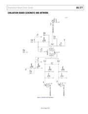
Figure 1 shows the bare evaluation board, component side and
circuit side. Figure 2 shows the evaluation board schematic. The
PCB layout pattern for the PCB is shown in Figure 3 and Figure 4.
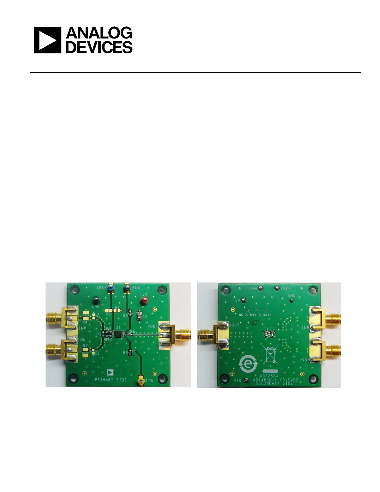
DIGITAL PICTURE OF EVALUATION BOARD
Figure 1. ADA4830-1BCP-EBZ Component Side (Primary) and Circuit Side (Secondary) of PCB
10543-001
SECONDARY SIDEPRIMARY SIDE
NOTES
1. THE
E
VALUATION BOARD SILKSCREEN PART NUMBER LABELING ON YOUR BOARD MAY BE DIFFERENT
FROM WHAT IS SHOWN HERE.
器件 Datasheet 文档搜索
AiEMA 数据库涵盖高达 72,405,303 个元件的数据手册,每天更新 5,000 多个 PDF 文件
