Datasheet 搜索 > 电压基准芯片 > ADI(亚德诺) > ADR3550WBRMZ-R7 数据手册 > ADR3550WBRMZ-R7 产品设计参考手册 1/20 页
 器件3D模型
¥ 1.607
ADR3550WBRMZ-R7 产品设计参考手册 - ADI(亚德诺)
制造商:
ADI(亚德诺)
分类:
电压基准芯片
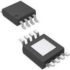
封装:
MSOP-8
描述:
微功耗,高精度 Micropower, High Accuracy
Pictures:
3D模型
符号图
焊盘图
引脚图
产品图
页面导航:
引脚图在P1P9Hot
原理图在P17
封装尺寸在P20
型号编码规则在P20
功能描述在P1P9
技术参数、封装参数在P1P3P8P20
应用领域在P1P18P19P20
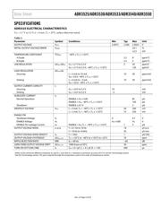
电气规格在P3P4P5P6P7P10

导航目录
ADR3550WBRMZ-R7数据手册
Page:
of 20 Go
若手册格式错乱,请下载阅览PDF原文件

Micropower, High Accuracy
Voltage References
Data Sheet
ADR3525/ADR3530/ADR3533/ADR3540/ADR3550
Rev. 0
Information furnished by Analog Devices is believed to be accurate and reliable. However, no
responsibility is assumed by Analog Devices for its use, nor for any infringements of patents or other
rights of third parties that may result from its use. Specifications subject to change without notice. No
license is granted by implication or otherwise under any patent or patent rights of Analog Devices.
Trademarks and registered trademarks are the property of their respective owners.
One Technology Way, P.O. Box 9106, Norwood, MA 02062-9106, U.S.A.
Tel: 781.329.4700 www.analog.com
Fax: 781.461.3113 ©2011 Analog Devices, Inc. All rights reserved.
FEATURES
Maximum temperature coefficient: 5 ppm/°C (B grade)
Low long-term drift (LTD): 30 ppm (initial 1 khr typical)
Initial output voltage error: ±0.1% (maximum)
Operating temperature range: −40°C to +125°C
Output current: +10 mA source/−3 mA sink
Low quiescent current: 100 μA (maximum)
Low dropout voltage: 250 mV at 2 mA
Output voltage noise (0.1 Hz to 10 Hz): 29 μV p-p at
4.096 V (typical)
Qualified for automotive applications
APPLICATIONS
Automotive battery monitors
Portable instrumentation
Process transmitters
Remote sensors
Medical instrumentation
PIN CONFIGURATION
09594-001
ENABLE
1
GND SENSE
2
GND FORCE
3
NC
4
V
IN
8
V
OUT
SENSE
7
V
OUT
FORCE
6
NC
5
NOTES
1. NC = NO CONNECT. DO NOT
CONNECT TO THIS PIN.
ADR35xx
TOP VIEW
(Not to Scale)
Figure 1. 8-Lead MSOP (RM-8 Suffix)
GENERAL DESCRIPTION
The ADR3525W, ADR3530W, ADR3533W, ADR3540W, and
ADR3550W are low cost, low power, high precision CMOS
voltage references, featuring a maximum temperature coeffi-
cient (TC) of 5 ppm/°C (B grade), 8 ppm/°C (A grade), low
operating current, and low output noise in an 8-lead MSOP
package. For high accuracy, the output voltage and temperature
coefficient are trimmed digitally during final assembly using the
Analog Devices, Inc., patented DigiTrim® technology.
The low output voltage hysteresis and low long-term output
voltage drift improve lifetime system accuracy.
These CMOS references are available in five output voltages, all
of which are specified over the automotive temperature range of
−40°C to +125°C.
Table 1. Selection Guide
Model Output Voltage (V) Input Voltage Range (V)
ADR3525W 2.500 2.7 to 5.5
ADR3530W 3.000 3.2 to 5.5
ADR3533W 3.300 3.5 to 5.5
ADR3540W 4.096 4.3 to 5.5
ADR3550W 5.000 5.2 to 5.5
器件 Datasheet 文档搜索
AiEMA 数据库涵盖高达 72,405,303 个元件的数据手册,每天更新 5,000 多个 PDF 文件
