Datasheet 搜索 > 微处理器 > TI(德州仪器) > AM3352BZCZD60 数据手册 > AM3352BZCZD60 产品设计参考手册 1/248 页
 器件3D模型
¥ 39.854
AM3352BZCZD60 产品设计参考手册 - TI(德州仪器)
制造商:
TI(德州仪器)
分类:
微处理器
封装:
LFBGA-324
描述:
TEXAS INSTRUMENTS AM3352BZCZD60 (受限产品), 芯片, 微处理器, SITARA CORTEX A8, 600MHZ, 324BGA
Pictures:
3D模型
符号图
焊盘图
引脚图
产品图
页面导航:
引脚图在P10Hot
原理图在P5P108P110P111P113P114P149P159P172
封装尺寸在P241P242P243P244
标记信息在P241P242P243P244
封装信息在P4P237P240P241P242P243P244P245
技术参数、封装参数在P2P80P81P82P83P84P85P86P87P88P89P90
应用领域在P4P88P245P248
电气规格在P49P89P90P91P92
导航目录
AM3352BZCZD60数据手册
Page:
of 248 Go
若手册格式错乱,请下载阅览PDF原文件

Product
Folder
Sample &
Buy
Technical
Documents
Tools &
Software
Support &
Community
Reference
Design
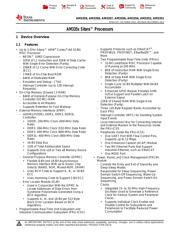
AM3359, AM3358, AM3357, AM3356, AM3354, AM3352, AM3351
SPRS717I –OCTOBER 2011–REVISED DECEMBER 2015
AM335x Sitara™ Processors
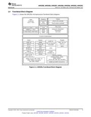
1 Device Overview
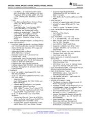
1.1 Features
1
– Supports Protocols such as EtherCAT
®
,
• Up to 1-GHz Sitara™ ARM
®
Cortex
®
-A8 32‑Bit
PROFIBUS, PROFINET, EtherNet/IP™, and
RISC Processor
More
– NEON™ SIMD Coprocessor
– Two Programmable Real-Time Units (PRUs)
– 32KB of L1 Instruction and 32KB of Data Cache
• 32-Bit Load/Store RISC Processor Capable
With Single-Error Detection (Parity)
of Running at 200 MHz
– 256KB of L2 Cache With Error Correcting Code
• 8KB of Instruction RAM With Single-Error
(ECC)
Detection (Parity)
– 176KB of On-Chip Boot ROM
• 8KB of Data RAM With Single-Error
– 64KB of Dedicated RAM
Detection (Parity)
– Emulation and Debug - JTAG
• Single-Cycle 32-Bit Multiplier With 64-Bit
– Interrupt Controller (up to 128 Interrupt
Accumulator
Requests)
• Enhanced GPIO Module Provides Shift-
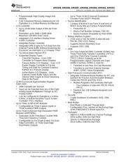
• On-Chip Memory (Shared L3 RAM)
In/Out Support and Parallel Latch on
– 64KB of General-Purpose On-Chip Memory
External Signal
Controller (OCMC) RAM
– 12KB of Shared RAM With Single-Error
– Accessible to All Masters
Detection (Parity)
– Supports Retention for Fast Wakeup
– Three 120-Byte Register Banks Accessible by
• External Memory Interfaces (EMIF)
Each PRU
– mDDR(LPDDR), DDR2, DDR3, DDR3L
– Interrupt Controller (INTC) for Handling System
Controller:
Input Events
• mDDR: 200-MHz Clock (400-MHz Data
– Local Interconnect Bus for Connecting Internal
Rate)
and External Masters to the Resources Inside
• DDR2: 266-MHz Clock (532-MHz Data Rate)
the PRU-ICSS
• DDR3: 400-MHz Clock (800-MHz Data Rate)
– Peripherals Inside the PRU-ICSS:
• DDR3L: 400-MHz Clock (800-MHz Data
• One UART Port With Flow Control Pins,
Rate)
Supports up to 12 Mbps
• 16-Bit Data Bus
• One Enhanced Capture (eCAP) Module
• 1GB of Total Addressable Space
• Two MII Ethernet Ports that Support
Industrial Ethernet, such as EtherCAT
• Supports One x16 or Two x8 Memory Device
Configurations
• One MDIO Port
– General-Purpose Memory Controller (GPMC)
• Power, Reset, and Clock Management (PRCM)
Module
• Flexible 8-Bit and 16-Bit Asynchronous
Memory Interface With up to Seven Chip
– Controls the Entry and Exit of Stand-By and
Selects (NAND, NOR, Muxed-NOR, SRAM)
Deep-Sleep Modes
• Uses BCH Code to Support 4-, 8-, or 16-Bit
– Responsible for Sleep Sequencing, Power
ECC
Domain Switch-Off Sequencing, Wake-Up
Sequencing, and Power Domain Switch-On
• Uses Hamming Code to Support 1-Bit ECC
Sequencing
– Error Locator Module (ELM)
– Clocks
• Used in Conjunction With the GPMC to
• Integrated 15- to 35-MHz High-Frequency
Locate Addresses of Data Errors from
Oscillator Used to Generate a Reference
Syndrome Polynomials Generated Using a
Clock for Various System and Peripheral
BCH Algorithm
Clocks
• Supports 4-, 8-, and 16-Bit per 512-Byte
• Supports Individual Clock Enable and
Block Error Location Based on BCH
Disable Control for Subsystems and
Algorithms
Peripherals to Facilitate Reduced Power
• Programmable Real-Time Unit Subsystem and
Consumption
Industrial Communication Subsystem (PRU-ICSS)
1
An IMPORTANT NOTICE at the end of this data sheet addresses availability, warranty, changes, use in safety-critical applications,
intellectual property matters and other important disclaimers. PRODUCTION DATA.
器件 Datasheet 文档搜索
AiEMA 数据库涵盖高达 72,405,303 个元件的数据手册,每天更新 5,000 多个 PDF 文件
