Datasheet 搜索 > FPGA芯片 > Altera(阿尔特拉) > EP3C40F484C8N 数据手册 > EP3C40F484C8N 产品设计参考手册 5/64 页
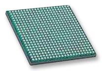
 器件3D模型
¥ 325.306
EP3C40F484C8N 产品设计参考手册 - Altera(阿尔特拉)
制造商:
Altera(阿尔特拉)
分类:
FPGA芯片
封装:
FBGA-484
Pictures:
3D模型
符号图
焊盘图
引脚图
产品图
页面导航:
引脚图在P18P20P23P27P42Hot
应用领域在P11
导航目录
EP3C40F484C8N数据手册
Page:
of 64 Go
若手册格式错乱,请下载阅览PDF原文件

Early System Planning Page 5
Cyclone III Design GuidelinesAugust 2013 Altera Corporation
Voltage deviation on the
VREF
pin can affect the threshold sensitivity for the input
operation. If a voltage referenced input is not utilized for a V
REF
group, the
VREF
pin is
released automatically by the Quartus II software for use as an I/O pin.
However, if the
VREF
pin is used as an I/O pin, it will have a higher pin capacitance
due to the power bus loading effects. The I/O edge rate will be slower than regular
I/O pins, which can affect the timing of the signal. For best results, do not use
VREF
pins as I/O pins when the
VREF
pins are part of a common bus or pin group that
requires similar timing characteristics. Similarly, do not use the
VREF
pins for clocks.
External Memory Interface
Cyclone III devices support interfaces to the DDR2 SDRAM, DDR SDRAM, and
QDRII SRAM. Depending on device density and package, specific side of I/O bank
may support up to x36 mode of memory interface. Supported modes in the
Cyclone III devices are x8, x9, x16, x18, x32, and x36 modes. Use the Pin Planner tool
to assist you in determining and making pin assignments for the memory interface.
In general, choose the top or bottom I/O banks instead of the side I/O banks to
achieve a higher clock rate for the external memory interfaces. The Cyclone III devices
support external memory interfaces up to 200 MHz.
f For more information about the DDR/DDR2 and QDRII pads placement, refer to the
Cyclone III Device I/O Feature chapter in the Cyclone III Device Handbook.
f For more information about the recommended design flow to implement the
DDR2 SDRAM memory interface with Cyclone III devices, refer to External Memory
Interface Handbook Volume 5, Section I. ALTMEMPHY Design.
f For a complete table of the maximum clock rate support across all speed grades for
every memory standard, refer to the External Memory Interfaces in the Cyclone III Device
Family chapter in the Cyclone III Device Handbook.
Pin-Out Files
The Cyclone III pin-out files contain information about the location for all the pins of
the devices, according to package:
■ For the I/O pins, you can find out which I/O bank and the V
REF
group the pins
belong to.
■ The pin-out files contain the description for the dedicated and multi-purpose pins.
■ The pin-out files help designer to determine the I/O pins to be used when creating
the design as well as when designing the board.
Apart from I/O pins, the location of dedicated and multi-purpose pins is also
important during the board design stage.
f To obtain device pin-outs for Cyclone III devices, refer to the Device Pin-Outs page of
the Literature section of the Altera website (www.altera.com).
器件 Datasheet 文档搜索
AiEMA 数据库涵盖高达 72,405,303 个元件的数据手册,每天更新 5,000 多个 PDF 文件
