Datasheet 搜索 > 地磁传感器 > ST Microelectronics(意法半导体) > LIS3MDLTR 数据手册 > LIS3MDLTR 产品设计参考手册 4/9 页
 器件3D模型
¥ 5.221
LIS3MDLTR 产品设计参考手册 - ST Microelectronics(意法半导体)
制造商:
ST Microelectronics(意法半导体)
分类:
地磁传感器
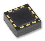
封装:
LGA-12
描述:
STMICROELECTRONICS LIS3MDLTR 模块, MEMS, 三轴磁强计, 1.9 V, 3.6 V, LGA, 12 引脚
Pictures:
3D模型
符号图
焊盘图
引脚图
产品图
LIS3MDLTR数据手册
Page:
of 9 Go
若手册格式错乱,请下载阅览PDF原文件

PCB design guidelines TN0018
4/9 DocID12707 Rev 6
2 PCB design guidelines
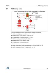
PCB land and solder mask general recommendations are shown in Figure 1. Refer to the
device datasheet for pad count, size and pitch.
It is recommended to open the solder mask external to the PCB land;
It is strongly recommended not to place any structure on the top metal layer
underneath the sensor (on the same side of the board). This must be defined as a
keepout area.
Traces connected to pads should be as much symmetric as possible. Symmetry and
balance for pad connection will help component self-alignment and will lead to better
control of solder paste reduction after reflow;
For optimal performance of the device, it is strongly recommended to place screw
mounting holes at a distance greater than 2 mm from the sensor.
If present, the pin #1 indicator must be left unconnected to ensure proper device
functionality.
In order to prevent noise coupling and thermo-mechanical stress, following standard
industry design practices for component placement is advised.
器件 Datasheet 文档搜索
AiEMA 数据库涵盖高达 72,405,303 个元件的数据手册,每天更新 5,000 多个 PDF 文件
