Datasheet 搜索 > National Semiconductor(美国国家半导体) > LM432MA/NOPB 数据手册 > LM432MA/NOPB 产品设计参考手册 3/5 页

 器件3D模型
¥ 1.452
LM432MA/NOPB 产品设计参考手册 - National Semiconductor(美国国家半导体)
制造商:
National Semiconductor(美国国家半导体)
封装:
SOIC
Pictures:
3D模型
符号图
焊盘图
引脚图
产品图
页面导航:
导航目录
LM432MA/NOPB数据手册
Page:
of 5 Go
若手册格式错乱,请下载阅览PDF原文件
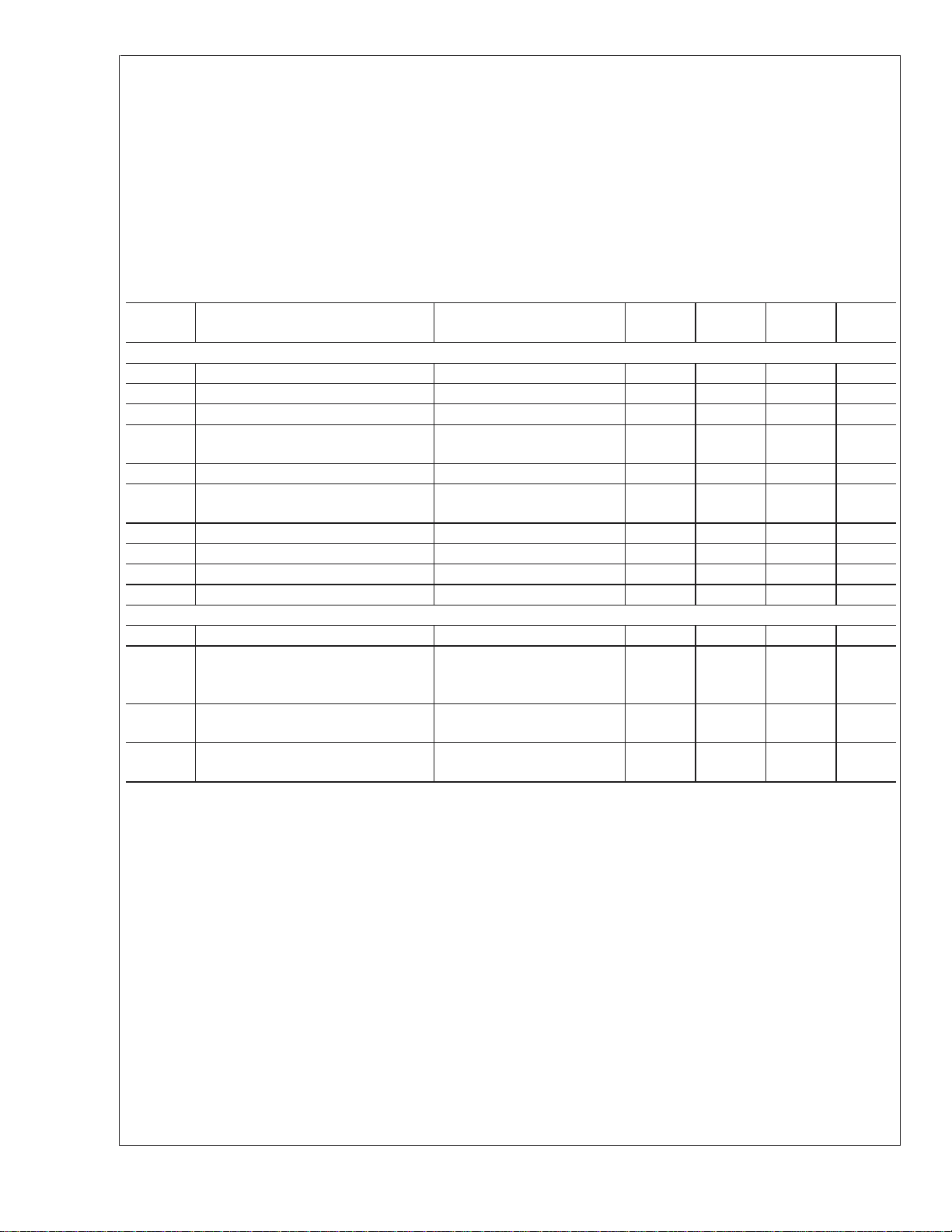
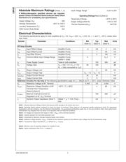
Absolute Maximum Ratings (Notes 1, 3)
If Military/Aerospace specified devices are required,
please contact the National Semiconductor Sales Office/
Distributors for availability and specifications.
Suppy Voltage (V
S
) 20V
Storage Temperature −65˚C to 150˚C
Junction Temperature (T
J
) 150˚C
ESD Human Body Model 2kV
Input Voltage Range −0.3V to 20V
Operating Ratings(Note 2),(Note 3)
Temperature Range −40˚C to 85˚C
Supply Voltage (Note 8) 2.5V to 16V
Thermal Resistance(θ
JA
) 162˚C/W
Electrical Characteristics
The following specifications apply for both amplifiers at V
S
= 5V, V
CM
= 2.5V, V
O
= 2.5V, R
L
=
∞
, and T
J
= 25˚C, unless other-
wise noted.
Symbol Parameter Conditions Min
(Note 5)
Typ
(Note 4)
Max
(Note 5)
Units
OP Amp Circuitry
V
OS
Input Offset Voltage Amplifier B only −4 0.6 4 mV
I
OS
Input Offset Current Amplifier B only 1 50 nA
I
B
Input Bias Current Amplifier B only 3 150 nA
V
CM
Common-Mode Input Voltage Range Amplifier B only,
CMRR
>
50dB
0V
S
-1 V
I
S
Power Supply Current Total for both amplifiers 150 500 µA
A
V
Voltage Gain V
S
= 16V, 1V
<
V
O
<
11V,
R
L
= 10kΩ connected to V
S
/2
65 100 dB
V
OL
Output Voltage Low 2 50 mV
V
OH
Output Voltage High V
S
– 1.5 V
S
– 1.3 V
I
SOURCE
Output Current Source 20 30 mA
I
SINK
Output Current Sink 5 11 mA
Reference Circuitry For Op Amp A The following specifications apply for I
Z
= 200µA and T
J
= 25˚C, unless otherwise noted.
V
Z
Reference Voltage at IN
+
Terminal 2.450 2.5 2.550 V
V
ZDEV
Reference Voltage Deviation at IN
+
Terminal Over Temperature
(Note 6),(Note 9)
−40˚C ≤ T
J
≤ 85˚C 4 65 mV
I
Z (MIN)
Minimum Cathode Current for
Regulation at IN
+
(V
Z
) Terminal
150 200 µA
r
z
Dynamic Output Impedance (Note 7) 200µA
<
I
Z
<
1mA, Freq =
0Hz
0.2 Ω
Note 1: Absolute Maximum Ratings indicate limits beyond which damage to the device may occur.
Note 2: Operating Rating indicate conditions for which the device is functional. These rating do not guarantee specific performance limits. For guaranteed
specifications and test conditions, see the Electrical Characteristics. The guaranteed specifications apply only for the test conditions listed. Some performance
characteristics may degrade when the device is not operated under the listed test conditions.
Note 3: All voltages are measured with respect to GND = 0V
DC
, unless otherwise specified.
Note 4: Typicals represent the most likely parametic norm.
Note 5: Guaranteed to National’s Average Outgoing Quality Level (AOQL).
Note 6: Reference voltage deviation, V
ZDEV
, is defined as the maximum variation of the reference input voltage over the full temperature range.
Note 7: The Dynamic Output Impendance, r
z
, is defined as r
z
= ∆V
Z
/∆I
Z
.
Note 8: Minimum value of operating voltage is for Amplifier B only.
Note 9: Typical Temperature drift ∆V/∆T = 12.8ppm/˚C
LM432
www.national.com 2
器件 Datasheet 文档搜索
AiEMA 数据库涵盖高达 72,405,303 个元件的数据手册,每天更新 5,000 多个 PDF 文件
