Datasheet 搜索 > 微处理器 > NXP(恩智浦) > LS1020AXE7MQB 数据手册 > LS1020AXE7MQB 产品设计参考手册 4/26 页
¥ 381.803
LS1020AXE7MQB 产品设计参考手册 - NXP(恩智浦)
制造商:
NXP(恩智浦)
分类:
微处理器
封装:
FCBGA-525
Pictures:
3D模型
符号图
焊盘图
引脚图
产品图
LS1020AXE7MQB数据手册
Page:
of 26 Go
若手册格式错乱,请下载阅览PDF原文件

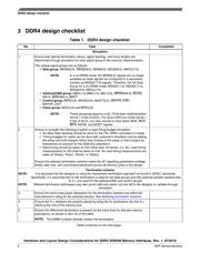
Table 1. DDR4 design checklist (continued)
No. Task Completed
NOTE:
The fly-by routing is recommended for address, command, control, and clock
signal bus.
21 Complete the following global routing items:
• Do not route any DDR4 signals over splits or voids.
• Ensure that traces routed near the edge of a reference plane maintain at least
30–40 mils gap to the edge of the reference plane.
• Allow no more than 1/2 of a trace width to be routed over via antipad.
22 Ensure the max lead-in trace length for data/address/command signals are no longer
than 7 inches.
Routing data bus
23 When routing the data lanes, route the outer-most (that is, the longest lane) first,
because this determines the amount of trace length to add on the inner data lanes.
24 Route all signals within a given byte lane on the same critical layer with the same via
count. Assuming ECC is used, the DDR4 data bus consists of nine data byte lanes.
NOTE:
The byte ordering below is not a requirement; byte lanes can be routed in the
order that best fits the customer design.
• Byte lane 0—MDQ(7:0), MDM(0), MDQS(0), MDQS(0)
• Byte lane 1—MDQ(15:8), MDM(1), MDQS(1), MDQS(1)
• Byte lane 2—MDQ(23:16), MDM(2), MDQS(2), MDQS(2)
• Byte lane 3—MDQ(31:24), MDM(3), MDQS(3), MDQS(3)
• Byte lane 4—MDQ(39:32), MDM(4), MDQS(4), MDQS(4)
• Byte lane 5—MDQ(47:40), MDM(5), MDQS(5), MDQS(5)
• Byte lane 6—MDQ(55:48), MDM(6), MDQS(6), MDQS(6)
• Byte lane 7—MDQ(63:56), MDM(7), MDQS(7), MDQS(7)
• Byte lane 8—MECC(7:0), MDM(8), MDQS(8), MDQS(8)
To facilitate fan-out of the DDR4 data lanes (if needed), alternate adjacent data lanes
onto different critical layers (see Figure 1 and Figure 2).
NOTE:
Some product implementations may only implement a 32-bit wide interface.
NOTE:
If the device supports ECC, NXP highly recommends that the user implements
ECC on the initial hardware prototypes.
25 Choose one of the following options to select the impedances and spacings for the
DDR4 data group.
Option #1 (wider traces—lower trace impedance):
• Single-ended impedance = 40 Ω. The lower impedance allows traces to be
slightly closer with less cross-talk.
• Utilize wider traces if stackup allows (7–8 mils).
• Spacing to other data signals = 1.5x to 2.0x
• Spacing to all other non-DDR signals = 4x
Option #2 (smaller traces—higher trace impedance):
• Single-ended impedance = 50 Ω
• Smaller trace widths (5–6 mils) can be used.
• Spacing between like signals should increase to 3x (for 5 mils) or 2.5x (for 6
mils), respectively.
26
Across all DDR4 data lanes:
• Ensure that all the data lanes are matched to within 2.0 inches.
27 Ensure bit and byte swapping rules are applied:
• Byte-swap is allowed in any order that would best fit the customer's design.
• No specific byte ordering is enforced or required.
Table continues on the next page...
DDR4 design checklist
Hardware and Layout Design Considerations for DDR4 SDRAM Memory Interfaces, Rev. 1, 07/2016
4 NXP Semiconductors
器件 Datasheet 文档搜索
AiEMA 数据库涵盖高达 72,405,303 个元件的数据手册,每天更新 5,000 多个 PDF 文件

