Datasheet 搜索 > 电压基准芯片 > Linear Technology(凌力尔特) > LT1790BIS6-3.3#TRMPBF 数据手册 > LT1790BIS6-3.3#TRMPBF 产品设计参考手册 5/26 页

¥ 15.73
LT1790BIS6-3.3#TRMPBF 产品设计参考手册 - Linear Technology(凌力尔特)
制造商:
Linear Technology(凌力尔特)
分类:
电压基准芯片
封装:
TSOT-23-6
Pictures:
3D模型
符号图
焊盘图
引脚图
产品图
页面导航:
典型应用电路图在P1P26
原理图在P24
封装尺寸在P3P25
焊盘布局在P25
型号编码规则在P3
标记信息在P3
封装信息在P3
技术参数、封装参数在P10
应用领域在P1P11P19P20P21P22P23
电气规格在P4P5P6P7P8P9P10P11P12P13P14P15
导航目录
LT1790BIS6-3.3#TRMPBF数据手册
Page:
of 26 Go
若手册格式错乱,请下载阅览PDF原文件
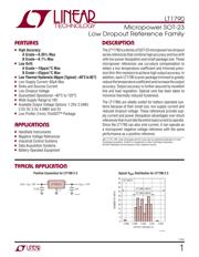
LT1790
5
1790fb
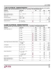
PARAMETER CONDITIONS MIN TYP MAX UNITS
Supply Current No Load
l
35 60
75
μA
μA
Minimum Operating Current—
Negative Output (See Figure 7)
V
OUT
= –1.25V, ±0.1% 100 125 μA
Turn-On Time C
LOAD
= 1μF 250 μs
Output Noise (Note 8) 0.1Hz ≤ f ≤ 10Hz
10Hz ≤ f ≤ 1kHz
10
14
μV
P-P
μV
RMS
Long-Term Drift of Output Voltage (Note 9) 50 ppm/√kHr
Hysteresis (Note 10) ΔT = 0°C to 70°C
ΔT = –40°C to 85°C
l
l
25
40
ppm
ppm
1.25V ELECTRICAL CHARACTERISTICS
The l denotes the specifi cations which apply over the specifi ed
temperature range, otherwise specifi cations are at T
A
= 25°C. C
L
= 1μF and V
IN
= 2.6V, unless otherwise noted.
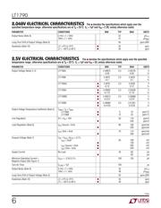
2.048V ELECTRICAL CHARACTERISTICS
The l denotes the specifi cations which apply over the
specifi ed temperature range, otherwise specifi cations are at T
A
= 25°C. C
L
= 1μF and V
IN
= 2.8V, unless otherwise noted.
PARAMETER CONDITIONS MIN TYP MAX UNITS
Output Voltage (Notes 3, 4) LT1790A 2.04697
–0.05
2.048 2.04902
0.05
V
%
LT1790B 2.04595
–0.1
2.048 2.05005
0.1
V
%
LT1790AC
l
l
2.04554
–0.12
2.048 2.05046
0.12
V
%
LT1790AI
l
l
2.04442
–0.175
2.048 2.05158
0.175
V
%
LT1790BC
l
l
2.04237
–0.275
2.048 2.05363
0.275
V
%
LT1790BI
l
l
2.03955
–0.4125
2.048 2.05645
0.4125
V
%
Output Voltage Temperature Coeffi cient (Note 5) T
MIN
≤ T
A
≤ T
MAX
LT1790A
LT1790B
l
l
5
12
10
25
ppm/°C
ppm/°C
Line Regulation 2.8V ≤ V
IN
≤ 18V
l
50 170
220
ppm/V
ppm/V
Load Regulation (Note 6) I
OUT
Source = 5mA
l
120 200
280
ppm/mA
ppm/mA
I
OUT
Sink = 3mA
l
130 260
450
ppm/mA
ppm/mA
Dropout Voltage (Note 7) V
IN
– V
OUT
, ΔV
OUT
= 0.1%
I
OUT
= 0mA
I
OUT
Source = 5mA
I
OUT
Sink = 3mA
l
l
l
50 100
500
750
450
mV
mV
mV
mV
Supply Current No Load
l
35 60
75
μA
μA
Minimum Operating Current—
Negative Output (See Figure 7)
V
OUT
= –2.048V, 0.1% 100 125 μA
Turn-On Time C
LOAD
= 1μF 350 μs
器件 Datasheet 文档搜索
AiEMA 数据库涵盖高达 72,405,303 个元件的数据手册,每天更新 5,000 多个 PDF 文件
