Datasheet 搜索 > PWM控制器 > ON Semiconductor(安森美) > NCP12510BSN65T1G 数据手册 > NCP12510BSN65T1G 产品设计参考手册 1/10 页

¥ 0.674
NCP12510BSN65T1G 产品设计参考手册 - ON Semiconductor(安森美)
制造商:
ON Semiconductor(安森美)
分类:
PWM控制器
封装:
TSOT-23-6
描述:
用于离线电源的电流模式PWM控制器
Pictures:
3D模型
符号图
焊盘图
引脚图
产品图
页面导航:
型号编码规则在P10
标记信息在P10
功能描述在P1
应用领域在P1
导航目录
NCP12510BSN65T1G数据手册
Page:
of 10 Go
若手册格式错乱,请下载阅览PDF原文件

© Semiconductor Components Industries, LLC, 2016
August, 2016 − Rev. 0
1 Publication Order Number:
EVBUM2485/D
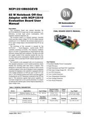
NCP12510B65GEVB
65 W Notebook Off-line
Adaptor with NCP12510
Evaluation Board User
Manual
Description
This evaluation board user manual describes the
NCP12510B65GEVB board and its main parameters, i.e.
efficiency, no−load input power consumption, EMI
signature, transient responses, etc.
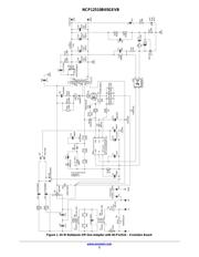
The evolution board is a flyback topology converter
which provides output voltage 19 Vdc for output nominal
current up to 3.5 A, therefore, the nominal output power is
65 W. Input voltage range is recommended from 90 Vac up
to 265 Vac.
The switching of the converter is ensured by the
NCP12510 – fixed−frequency current−mode PWM
controller switching at 65 kHz. The frequency foldback
down to 26 kHz is implemented for achievement the high
efficiency during light load conditions. The skip cycle and
low supply current of the controller ensures the very low
no−load input power consumption (standby power) of the
converter, which is less than 40 mW without indication LED
on output.
The controller is also equipped with a lot of protections.
The standard protection is over−current protection which
disables the switching after fault timer is elapsed. This
protection is activated when over−current or short−circuit
conditions appear. In the case of damage of some component
important for regulation, the controller is equipped with fast
over−voltage protection on OPP pin (pin 3) and VCC pin
(pin 5). The controller protects the whole converter against
overheating by an NTC thermistor connected to the OPP pin
(pin 3). The protection against high power capability of
converter at high line is over−power protection. It is based
on reducing the internal peak current setpoint depending on
input voltage value.
Key Features
• Excellent Standby Power Consumption
• High Efficiency
• High Robustness and High ESD Capabilities
• Wide Input Voltage Range (90 – 265 Vac)
• Low EMI Emissions
• Over−Current Protection
• Over−Temperature Protection
• Over−Voltage Protection
• Over−Power Protection
Table 1. GENERAL PARAMETERS
Device Applications Input Voltage
Nominal Output
Voltage / Current
Output
Power
V
OUT
Ripple
NCP12510 Notebook Adaptors, Ac – dc
converters for consumer electronics
90 – 265 Vac 19 Vdc / 3.5 A
4.5 A max limit
65 W < 20 mV @ no load
and min input voltage
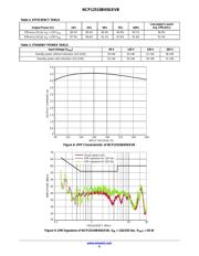
Efficiency Standby Power
Operating
Temperature
Cooling Topology Board Size
~91% 20 mW @ 120 Vac
31 mW @ 230 Vac
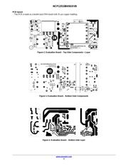
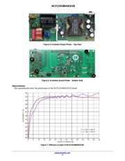
0 – 50°C Passive cooling Flyback 111 x 48 x 21 mm
www.onsemi.com
EVAL BOARD USER’S MANUAL
器件 Datasheet 文档搜索
AiEMA 数据库涵盖高达 72,405,303 个元件的数据手册,每天更新 5,000 多个 PDF 文件
