Datasheet 搜索 > 电压基准芯片 > TI(德州仪器) > TL431AILPR 数据手册 > TL431AILPR 产品设计参考手册 1/18 页

¥ 0.268
TL431AILPR 产品设计参考手册 - TI(德州仪器)
制造商:
TI(德州仪器)
分类:
电压基准芯片
封装:
TO-226-3
描述:
TEXAS INSTRUMENTS TL431AILPR. 芯片, 可调并联电压基准, 2.495V, 1%, TO-92, 整卷
Pictures:
3D模型
符号图
焊盘图
引脚图
产品图
页面导航:
典型应用电路图在P7
原理图在P2
封装尺寸在P15P16P17P18
焊盘布局在P17P18
型号编码规则在P1P13P14P18
标记信息在P1P13P14P18
封装信息在P13P14
技术参数、封装参数在P13P14
应用领域在P1P7P11P13P14
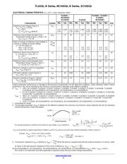
电气规格在P3P4
型号编号列表在P2
导航目录
TL431AILPR数据手册
Page:
of 18 Go
若手册格式错乱,请下载阅览PDF原文件
© Semiconductor Components Industries, LLC, 1995
October, 2016 − Rev. 39
1 Publication Order Number:
TL431/D
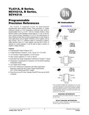
TL431A, B Series,
NCV431A, B Series,
SCV431A
Programmable
Precision References
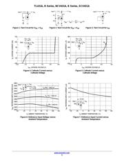
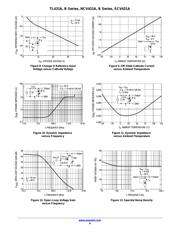
The TL431A, B integrated circuits are three−terminal
programmable shunt regulator diodes. These monolithic IC voltage
references operate as a low temperature coefficient zener which is
programmable from V
ref
to 36 V with two external resistors. These
devices exhibit a wide operating current range of 1.0 mA to 100 mA
with a typical dynamic impedance of 0.22 W. The characteristics of
these references make them excellent replacements for zener diodes in
many applications such as digital voltmeters, power supplies, and op
amp circuitry. The 2.5 V reference makes it convenient to obtain a
stable reference from 5.0 V logic supplies, and since the TL431A, B
operates as a shunt regulator, it can be used as either a positive or
negative voltage reference.
Features
• Programmable Output Voltage to 36 V
• Voltage Reference Tolerance: ±0.4%, Typ @ 25°C (TL431B)
• Low Dynamic Output Impedance, 0.22 W Typical
• Sink Current Capability of 1.0 mA to 100 mA
• Equivalent Full−Range Temperature Coefficient of 50 ppm/°C Typical
• Temperature Compensated for Operation over Full Rated Operating
Temperature Range
• Low Output Noise Voltage
• NCV/SCV Prefixes for Automotive and Other Applications
Requiring Unique Site and Control Change Requirements;
AEC−Q100 Qualified and PPAP Capable
• These Devices are Pb−Free, Halogen Free/BFR Free and are RoHS
Compliant
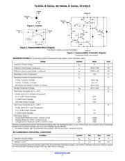
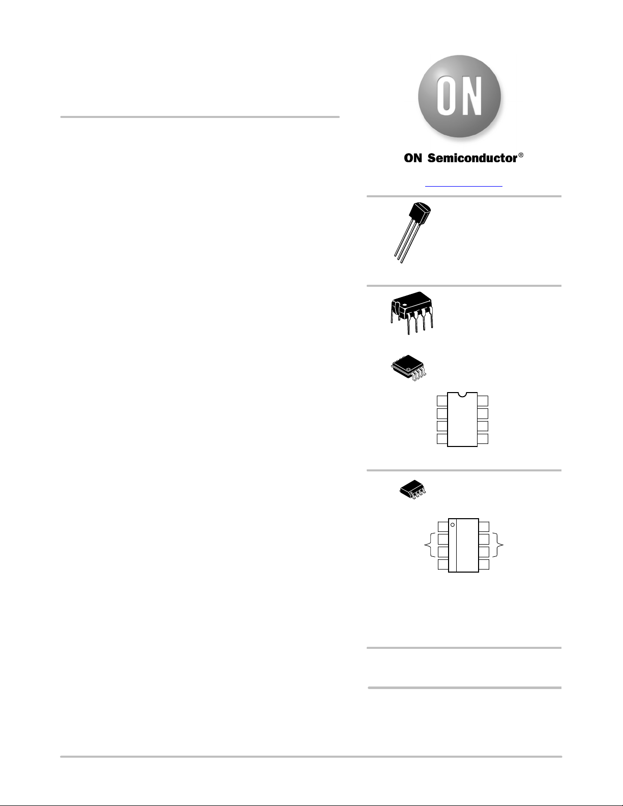
(Top View)
3
1
Reference
N/C
N/C
N/C
2
4
8
7
6
5
N/C
Anode
N/C
Cathode
Anode Anode
TO−92 (TO−226)
LP SUFFIX
CASE 29
PDIP−8
P SUFFIX
CASE 626
SOIC−8
D SUFFIX
CASE 751
Pin 1. Reference
2. Anode
3. Cathode
(Top View)
3
1
Reference
N/C
2
4
8
7
6
5
N/C
Cathode
Micro8E
DM SUFFIX
CASE 846A
8
1
8
1
1
2
3
This is an internally modified SOIC−8 package. Pins 2, 3, 6 an
d
7 are electrically common to the die attach flag. This interna
l
lead frame modification increases power dissipation capabilit
y
when appropriately mounted on a printed circuit board. Th
is
modified package conforms to all external dimensions of th
e
standard SOIC−8 package.
See detailed ordering and shipping information on page 13 o
f
this data sheet.
ORDERING INFORMATION
See general marking information in the device marking
section on page 14 of this data sheet.
DEVICE MARKING INFORMATION
www.onsemi.com
器件 Datasheet 文档搜索
AiEMA 数据库涵盖高达 72,405,303 个元件的数据手册,每天更新 5,000 多个 PDF 文件
