Datasheet 搜索 > 逻辑控制器 > TI(德州仪器) > TWL1200YFFR 数据手册 > TWL1200YFFR 产品设计参考手册 1/12 页

¥ 5.561
TWL1200YFFR 产品设计参考手册 - TI(德州仪器)
制造商:
TI(德州仪器)
分类:
逻辑控制器
封装:
UFBGA-49
描述:
SDIO , UART和音频电压转换收发器 SDIO, UART, AND AUDIO VOLTAGE-TRANSLATION TRANSCEIVER
Pictures:
3D模型
符号图
焊盘图
引脚图
产品图
页面导航:
原理图在P10
焊盘布局在P2P3P4P5P6P7P8P9P10P11
功能描述在P2
应用领域在P12
导航目录
TWL1200YFFR数据手册
Page:
of 12 Go
若手册格式错乱,请下载阅览PDF原文件
Application Report
SCEA042 – July 2009
TWL1200 PCB Design Guidelines
Jason Battle ................................................................................................. Standard Linear and Logic
ABSTRACT
The Texas Instruments TWL1200 is a 19-bit voltage translator specifically designed to
bridge the 1.8-V/2.6-V digital-switching compatibility gap between a 2.6-V baseband
and the Wi-Link-6 (WL1271/3), and is optimized for SDIO, UART, and audio functions.
When laying out a printed circuit board (PCB) for the TWL1200, careful consideration of
design rules and guidelines must be employed to help preserve signal integrity and
ensure optimal device performance.
This document presents several guidelines for designing the TWL1200 PCB and
includes recommendations for device placement and proper layout.
Contents
1 Overview ............................................................................................. 2
2 Layout and Design Guidelines .................................................................... 2
3 TWL1200 Reference Design Schematic ....................................................... 10
4 References ......................................................................................... 11
List of Figures
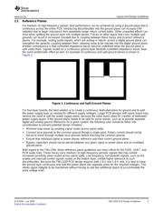
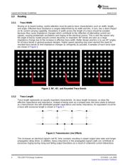
1 Continuous and Split Ground Planes ............................................................ 3
2 90 ° , 45 ° , and Rounded Trace Bends ............................................................ 4
3 Transmission Line Effects ......................................................................... 4
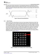
4 Power and Ground Rail Bounce .................................................................. 5
5 Leadaway Trace Routing for BGA or WCSP Packages ....................................... 5
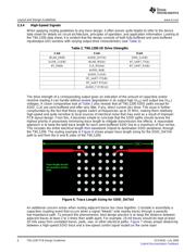
6 Trace Length Sizing for SDIO_DATA0 .......................................................... 6
7 Proper High-Speed Trace Routing for Crosstalk Reduction .................................. 7
8 Cross-Sectional View of Blind, Buried, and Traditional Vias .................................. 8
9 250- µ m and 150- µ m Via Sizing for TWL1200 and WL1271/3 Pads ......................... 8
10 Proper TWL1200 Power Supply Decoupling .................................................... 9
11 TWL1200 Reference Design .................................................................... 10
List of Tables
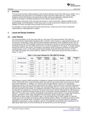
1 Four-Layer Stackup for TWL1200 PCB Design ................................................ 2
2 TWL1200 I/O Drive Strengths..................................................................... 6
SCEA042 – July 2009 TWL1200 PCB Design Guidelines 1
Submit Documentation Feedback
器件 Datasheet 文档搜索
AiEMA 数据库涵盖高达 72,405,303 个元件的数据手册,每天更新 5,000 多个 PDF 文件
